What are the Layers in a PCB?
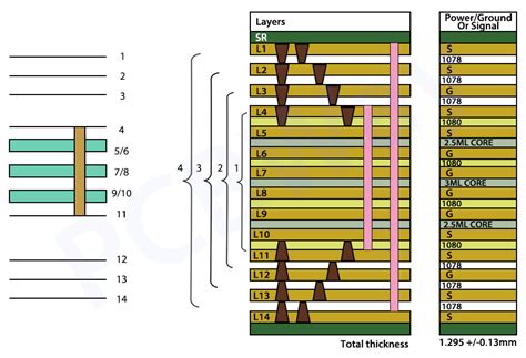
A printed circuit board (PCB) is a fundamental component in modern electronics that mechanically supports and electrically connects electronic components using conductive tracks, pads, and other features etched from copper sheets laminated onto a non-conductive substrate. PCBs can be single-sided (one copper layer), double-sided (two copper layers on both sides of one substrate layer), or multi-layered (outer and inner layers of copper, alternating with layers of substrate).
The number of layers in a PCB varies depending on the complexity and requirements of the circuit design. The most common PCB configurations are:
- Single-layer PCB: one conductive layer
- Double-layer PCB: two conductive layers
- Multi-layer PCB: three or more conductive layers
In this article, we will focus on the 7 working layers typically found in a multi-layer PCB and their functions.
Table 1: Overview of PCB Layers
| Layer | Name | Function |
|---|---|---|
| 1 | Top Layer | Contains components and routing |
| 2 | Ground Plane | Provides a low-impedance ground reference |
| 3 | Power Plane | Distributes power to components |
| 4 | Signal Layer 1 | Routes signals between components |
| 5 | Signal Layer 2 | Additional signal routing layer |
| 6 | Power Plane | Additional power distribution layer |
| 7 | Bottom Layer | Contains components and routing |
The Top Layer
The top layer, also known as the component layer, is the outermost layer of the PCB where most of the electronic components are placed and soldered. This layer contains the majority of the conductive traces that connect the components together, forming the desired circuit.
Key features of the top layer include:
- Component footprints: The top layer contains the land patterns or footprints for surface-mounted devices (SMDs) and through-hole components.
- Silkscreen: The top layer also includes silkscreen, which is a printed overlay that provides text, logos, and other identifying marks for easier assembly and troubleshooting.
- Solder mask: A protective coating called solder mask is applied over the copper traces, leaving only the exposed pads for soldering components.
Best practices for top layer design:
- Place components strategically to minimize trace lengths and crossovers.
- Ensure adequate spacing between components for proper soldering and heat dissipation.
- Use clear and concise silkscreen labels for easy identification of components and connectors.
The Ground Plane
The ground plane is a conductive layer that provides a low-impedance reference point for the circuit’s ground. It helps to reduce electromagnetic interference (EMI), minimizes ground loops, and improves signal integrity by providing a stable reference voltage.
Key features of the ground plane include:
- Solid copper pour: The ground plane is typically a solid copper pour that covers most of the PCB area, with clearances around through-holes and vias.
- Stitching vias: Stitching vias are used to connect the ground plane to ground planes on other layers, ensuring a low-impedance path for return currents.
Best practices for ground plane design:
- Keep the ground plane as continuous as possible, avoiding unnecessary splits or cuts.
- Use an appropriate number of stitching vias to maintain a low-impedance connection between ground planes on different layers.
- Provide adequate clearance around high-speed signals to minimize crosstalk and EMI.

The Power Plane
The power plane is a conductive layer dedicated to distributing power to the components on the PCB. It provides a low-impedance path for the power supply, minimizing voltage drops and ensuring stable power delivery.
Key features of the power plane include:
- Solid copper pour: Like the ground plane, the power plane is typically a solid copper pour covering most of the PCB area.
- Split planes: In some cases, the power plane may be split into multiple sections to accommodate different voltage levels or to isolate sensitive circuits.
Best practices for power plane design:
- Ensure the power plane has sufficient copper thickness to handle the required current.
- Use appropriate decoupling capacitors near power-hungry components to minimize voltage fluctuations.
- Consider split planes for circuits with multiple voltage levels or sensitive analog sections.
Signal Layers
Signal layers are conductive layers dedicated to routing signals between components on the PCB. In a 7-layer PCB, there are typically two signal layers (Signal Layer 1 and Signal Layer 2) that provide additional routing space for complex circuits.
Key features of signal layers include:
- Trace routing: Signal layers contain the conductive traces that carry signals between components, following specific design rules for width, spacing, and topology.
- Vias: Vias are used to connect traces on different layers, allowing signals to traverse the PCB vertically.
Best practices for signal layer design:
- Follow controlled impedance guidelines for high-speed signals to maintain signal integrity.
- Minimize crosstalk by providing adequate spacing between traces and using appropriate trace geometries.
- Use vias strategically to minimize signal reflections and maintain a clean signal path.
The Bottom Layer
The bottom layer is similar to the top layer, serving as a secondary component layer for additional component placement and routing. In some cases, the bottom layer may be used primarily for routing, with fewer components placed on this side of the board.
Key features of the bottom layer include:
- Component footprints: Like the top layer, the bottom layer contains land patterns for SMDs and through-hole components.
- Routing: The bottom layer provides additional space for routing traces, helping to minimize congestion on the top layer.
- Solder mask and silkscreen: The bottom layer also includes solder mask and silkscreen for protection and identification.
Best practices for bottom layer design:
- Consider the assembly process when placing components on the bottom layer, ensuring accessibility for soldering and inspection.
- Use the bottom layer for routing, especially for signals that do not have strict impedance or timing requirements.
- Provide clear silkscreen markings for any components or connectors on the bottom layer.
Frequently Asked Questions (FAQ)
1. What is the purpose of having multiple layers in a PCB?
Multiple layers in a PCB provide several benefits:
- Increased routing space for complex circuits
- Better power and ground distribution
- Improved signal integrity and reduced EMI
- Compact board design due to higher component density
2. How do vias connect different layers in a PCB?
Vias are conductive holes drilled through the PCB that allow signals to travel between layers. They are typically plated with copper to ensure a reliable electrical connection. There are several types of vias, including through-hole vias, blind vias, and buried vias, each with specific applications depending on the PCB design requirements.
3. What is controlled impedance, and why is it important for high-speed signals?
Controlled impedance refers to the precise management of a trace’s impedance to match the impedance of the source and load. This is crucial for high-speed signals, as impedance mismatches can cause signal reflections, leading to signal integrity issues such as ringing, overshoot, and undershoot. By designing traces with controlled impedance, these issues can be minimized, ensuring reliable high-speed signal transmission.
4. How does the ground plane help reduce EMI and improve signal integrity?
The ground plane provides a low-impedance return path for currents, which helps to minimize ground loops and reduce electromagnetic interference (EMI). By maintaining a stable reference voltage, the ground plane also improves signal integrity by reducing noise and crosstalk between signals. A continuous ground plane with proper stitching vias ensures that return currents flow directly beneath their corresponding signals, minimizing loop area and reducing EMI.
5. What are split power planes, and when are they used?
Split power planes are power planes divided into multiple sections to accommodate different voltage levels or to isolate sensitive circuits. They are used in PCBs with multiple power domains, such as those containing both digital and analog circuits or devices requiring different operating voltages. By splitting the power plane, you can prevent noise coupling between different sections of the board and ensure stable power delivery to each part of the circuit.
Conclusion
Understanding the 7 working layers in a printed circuit board is essential for designing reliable and high-performance electronic devices. Each layer serves a specific purpose, from component placement and routing to power distribution and signal integrity. By following best practices for each layer and considering the overall PCB stack-up, designers can create robust and efficient PCBs that meet the requirements of modern electronic applications.
As PCB technology continues to evolve, designers must stay up-to-date with the latest techniques and materials to ensure their designs remain competitive and reliable. By mastering the principles of PCB layer design, engineers can push the boundaries of electronic innovation and create cutting-edge products that shape our future.
Leave a Reply