Introduction to PCB Thickness
Printed Circuit Boards (PCBs) are the backbone of modern electronics. They provide a platform for mounting and connecting electronic components, enabling the creation of complex circuits in a compact and efficient manner. One of the critical factors in PCB design and manufacturing is the thickness of the board. PCB thickness plays a crucial role in determining the mechanical strength, thermal management, and electrical performance of the circuit board.
In this article, we will dive deep into the world of standard PCB thickness, exploring the various factors that influence the choice of thickness, the common thickness options available, and the impact of thickness on PCB performance. We will also discuss the manufacturing processes involved in creating PCBs of different thicknesses and provide insights into the best practices for selecting the appropriate thickness for your specific application.
Factors Influencing PCB Thickness Selection
When deciding on the thickness of a PCB, several factors need to be considered to ensure optimal performance and reliability. These factors include:
1. Application Requirements
The intended application of the PCB is one of the primary factors that determine the appropriate thickness. Different applications have varying demands in terms of mechanical strength, thermal management, and electrical performance. For example, a PCB designed for a high-power application may require a thicker board to dissipate heat effectively, while a PCB for a lightweight, portable device may prioritize a thinner board to minimize weight and size.
2. Layer Count
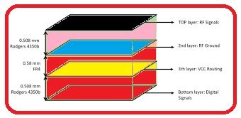
The number of layers in a PCB also influences the choice of thickness. As the layer count increases, the overall thickness of the board typically increases as well. This is because each additional layer requires its own substrate and copper foil, adding to the total thickness of the board. However, advancements in PCB manufacturing technologies have enabled the production of high-layer-count boards with relatively thin profiles.
3. Mechanical Strength
The mechanical strength of a PCB is directly related to its thickness. Thicker boards offer greater rigidity and resistance to bending and warping, making them suitable for applications that require robust mechanical performance. On the other hand, thinner boards are more flexible and can be used in applications where conformity to a specific shape or space is necessary.
4. Thermal Management
PCB thickness also plays a significant role in thermal management. Thicker boards have a higher thermal mass and can dissipate heat more effectively than thinner boards. This is particularly important in high-power applications where efficient heat dissipation is critical to prevent component failure and ensure reliable operation.
5. Electrical Performance
The thickness of a PCB can impact its electrical performance, particularly in high-frequency applications. Thinner boards have lower dielectric losses and can support higher signal speeds compared to thicker boards. However, thinner boards also have higher impedance and may be more susceptible to signal integrity issues, such as crosstalk and electromagnetic interference (EMI).
6. Manufacturing Constraints
PCB manufacturing capabilities and constraints also influence the choice of thickness. Some manufacturers may have limitations on the minimum or maximum thickness they can produce, depending on their equipment and processes. Additionally, certain manufacturing techniques, such as high-density interconnect (HDI) or microvias, may have specific thickness requirements to ensure reliable fabrication.

Common PCB Thickness Options
PCB thickness is typically measured in either millimeters (mm) or mils (thousands of an inch). The most common PCB thickness options are:
1. 0.8mm (31.5 mils)
- Thin and lightweight
- Suitable for portable and space-constrained applications
- Commonly used in mobile devices, wearables, and small consumer electronics
2. 1.0mm (39.4 mils)
- Slightly thicker than 0.8mm
- Offers a balance between mechanical strength and flexibility
- Used in a wide range of applications, including consumer electronics and industrial controls
3. 1.2mm (47.2 mils)
- Thicker and more rigid than 1.0mm
- Provides enhanced mechanical strength and thermal management
- Often used in automotive electronics, power supplies, and high-reliability applications
4. 1.6mm (63.0 mils)
- One of the most common PCB thicknesses
- Offers excellent mechanical strength and thermal performance
- Widely used in industrial, automotive, and aerospace applications
5. 2.0mm (78.7 mils)
- Thicker and more robust than 1.6mm
- Provides superior mechanical strength and heat dissipation
- Used in high-power applications, such as power electronics and motor controls
6. 2.4mm (94.5 mils) and above
- Extremely thick and rigid
- Offers the highest level of mechanical strength and thermal management
- Used in specialized applications, such as heavy-duty industrial equipment and military electronics
Table 1 summarizes the common PCB thickness options and their typical applications:
| Thickness | Mils | Applications |
|---|---|---|
| 0.8mm | 31.5 mils | Portable devices, wearables, small consumer electronics |
| 1.0mm | 39.4 mils | Consumer electronics, industrial controls |
| 1.2mm | 47.2 mils | Automotive electronics, power supplies, high-reliability |
| 1.6mm | 63.0 mils | Industrial, automotive, aerospace |
| 2.0mm | 78.7 mils | High-power applications, power electronics, motor controls |
| 2.4mm+ | 94.5 mils+ | Heavy-duty industrial equipment, military electronics |

Impact of PCB Thickness on Performance
The thickness of a PCB has a direct impact on its performance in various aspects. Let’s explore how PCB thickness affects mechanical strength, thermal management, and electrical performance.
Mechanical Strength
As mentioned earlier, thicker PCBs offer greater mechanical strength and rigidity compared to thinner boards. This is particularly important in applications where the PCB is subject to physical stress, vibrations, or shock. Thicker boards are less likely to bend, warp, or crack under these conditions, ensuring reliable operation and longevity of the circuit.
However, it’s important to note that the mechanical strength of a PCB is not solely determined by its thickness. Other factors, such as the material composition of the substrate, the copper weight, and the presence of reinforcing materials like fiberglass, also contribute to the overall mechanical performance of the board.
Thermal Management
PCB thickness plays a crucial role in thermal management, especially in high-power applications where efficient heat dissipation is essential. Thicker boards have a higher thermal mass and conductivity, allowing them to spread and dissipate heat more effectively than thinner boards.
When a component generates heat on a PCB, the heat is conducted through the copper traces and the substrate to the surrounding environment. A thicker board provides a larger cross-sectional area for heat conduction, reducing thermal resistance and improving heat transfer. This helps in preventing hot spots and thermal stress on components, enhancing the overall reliability and lifespan of the circuit.
Moreover, thicker boards offer more options for thermal management techniques, such as the use of thermal vias, heat sinks, and metal core substrates. These techniques further enhance the heat dissipation capabilities of the PCB, ensuring optimal thermal performance.
Electrical Performance
PCB thickness has a significant impact on the electrical performance of the circuit, particularly in high-frequency applications. Thinner boards generally have better electrical characteristics compared to thicker boards.
At high frequencies, the dielectric constant (Dk) and dissipation factor (Df) of the substrate material become critical. A lower Dk value results in faster signal propagation and reduced signal loss, while a lower Df value minimizes signal attenuation and power dissipation. Thinner boards typically have lower Dk and Df values, making them suitable for high-speed and high-frequency applications.
However, thinner boards also have higher impedance and may be more susceptible to signal integrity issues, such as crosstalk and electromagnetic interference (EMI). The reduced distance between the copper traces on a thinner board can lead to increased coupling and interference between signals. To mitigate these issues, careful design considerations, such as proper trace routing, impedance matching, and the use of shielding techniques, are necessary.
On the other hand, thicker boards offer better power handling capabilities and lower impedance, making them suitable for high-current and low-frequency applications. The increased thickness allows for wider traces and larger copper areas, reducing resistance and improving current carrying capacity.

Manufacturing Processes for Different PCB Thicknesses
The manufacturing process for PCBs varies depending on the desired thickness and the specific requirements of the application. Let’s explore the common manufacturing processes used for creating PCBs of different thicknesses.
Standard PCB Manufacturing Process
The standard PCB manufacturing process involves several steps, including:
-
Substrate preparation: The base material, typically a fiberglass-reinforced epoxy laminate, is cut to the required size and shape.
-
Copper foil lamination: Copper foil is laminated onto the substrate using heat and pressure.
-
Drilling: Holes are drilled through the board to accommodate components and vias.
-
Plating: The drilled holes are plated with copper to create electrical connections between layers.
-
Patterning: The copper foil is patterned using photolithography and etching techniques to create the desired circuit layout.
-
Solder mask application: A protective solder mask is applied to the board, leaving exposed areas for component soldering.
-
Surface finishing: The exposed copper areas are coated with a surface finish, such as HASL (Hot Air Solder Leveling) or ENIG (Electroless Nickel Immersion Gold), to prevent oxidation and improve solderability.
This standard process can produce PCBs with thicknesses ranging from 0.8mm to 2.4mm and above, depending on the number of layers and the specific requirements of the application.
High-Density Interconnect (HDI) Manufacturing
High-Density Interconnect (HDI) manufacturing is a advanced PCB fabrication technique that enables the production of boards with finer traces, smaller vias, and higher layer counts in a thinner profile. HDI PCBs typically have a thickness of 0.8mm or less and can accommodate a higher density of components and interconnects.
The HDI manufacturing process involves the use of microvias, which are small, laser-drilled holes that connect the outer layers to the inner layers of the board. These microvias allow for shorter signal paths and reduced signal loss, making HDI PCBs suitable for high-speed and high-frequency applications.
The HDI manufacturing process includes additional steps compared to the standard process, such as:
-
Microvia drilling: Laser drilling is used to create small, precise holes in the outer layers of the board.
-
Copper filling: The microvias are filled with copper using a special plating process to create reliable electrical connections.
-
Sequential lamination: Multiple layers of the board are laminated together in a sequential manner, allowing for the creation of complex, multi-layer designs.
HDI manufacturing enables the production of high-performance, compact PCBs with improved signal integrity and reduced EMI.
Flexible PCB Manufacturing
Flexible PCBs, also known as flex circuits, are designed to bend and flex without damaging the electrical connections. These PCBs are typically thinner than standard rigid boards, with thicknesses ranging from 0.1mm to 0.5mm.
The manufacturing process for flexible PCBs differs from rigid boards in several aspects:
-
Substrate material: Flexible substrates, such as polyimide or polyester films, are used instead of rigid fiberglass laminates.
-
Adhesive lamination: The copper foil is laminated onto the flexible substrate using a special adhesive that allows for flexibility.
-
Coverlay application: A protective coverlay film is applied to the flex circuit to provide insulation and mechanical protection.
Flexible PCBs offer unique advantages, such as the ability to conform to irregular shapes, reduced weight and space requirements, and improved resistance to vibrations and shocks.
Best Practices for Selecting PCB Thickness
When selecting the appropriate PCB thickness for your application, consider the following best practices:
-
Understand the application requirements: Clearly define the mechanical, thermal, and electrical requirements of your application to guide your thickness selection.
-
Consider the layer count: Determine the number of layers needed to accommodate your circuit design and choose a thickness that supports the desired layer count.
-
Evaluate the mechanical demands: Assess the expected physical stresses, vibrations, and shocks that the PCB will be subjected to and select a thickness that provides adequate mechanical strength.
-
Analyze the thermal management needs: Consider the power dissipation requirements of your components and choose a thickness that enables efficient heat transfer and thermal management.
-
Assess the electrical performance requirements: Evaluate the signal speed, frequency, and integrity demands of your application and select a thickness that minimizes signal loss and interference.
-
Consult with PCB manufacturers: Engage with experienced PCB manufacturers to discuss your specific requirements and obtain guidance on the most suitable thickness options for your application.
-
Prototype and test: Before finalizing your design, prototype and test your PCB to validate its performance and make any necessary adjustments to the thickness or other design parameters.
By following these best practices and carefully considering the factors that influence PCB thickness selection, you can ensure that your PCB design meets the specific requirements of your application while optimizing performance, reliability, and manufacturability.
FAQ
- What is the most common PCB thickness?
-
The most common PCB thickness is 1.6mm (63.0 mils). This thickness offers a good balance between mechanical strength, thermal management, and electrical performance, making it suitable for a wide range of applications.
-
Can I use a thinner PCB for high-power applications?
-
While it is possible to use a thinner PCB for high-power applications, it is generally recommended to use a thicker board (1.6mm or above) to ensure better thermal management and power handling capabilities. Thicker boards have a higher thermal mass and conductivity, allowing for more efficient heat dissipation and reducing the risk of thermal stress on components.
-
What is the minimum PCB thickness available?
-
The minimum PCB thickness available depends on the manufacturing capabilities of the PCB fabricator. Some advanced manufacturing techniques, such as High-Density Interconnect (HDI), can produce PCBs as thin as 0.4mm (15.7 mils) or even thinner. However, for most standard PCB applications, the minimum thickness is typically around 0.8mm (31.5 mils).
-
How does PCB thickness affect signal integrity?
-
PCB thickness can have a significant impact on signal integrity, especially in high-frequency applications. Thinner boards generally have better electrical characteristics, such as lower dielectric constant (Dk) and dissipation factor (Df), which result in faster signal propagation and reduced signal loss. However, thinner boards may also be more susceptible to crosstalk and electromagnetic interference (EMI) due to the reduced distance between copper traces.
-
Can I mix different PCB thicknesses in the same design?
- Yes, it is possible to mix different PCB thicknesses in the same design using a technique called “stepped” or “sculpted” PCBs. This approach involves varying the thickness of the board in specific areas to accommodate different components or to optimize thermal management and mechanical strength. However, designing and manufacturing stepped PCBs requires careful planning and coordination with the PCB fabricator to ensure compatibility and manufacturability.
Conclusion
PCB thickness is a critical factor in the design and manufacturing of printed circuit boards. It influences the mechanical strength, thermal management, and electrical performance of the board, and plays a crucial role in determining the overall reliability and functionality of the electronic device.
When selecting the appropriate PCB thickness for your application, it is essential to consider the specific requirements and constraints of your design. Factors such as the intended application, layer count, mechanical demands, thermal management needs, and electrical performance requirements should be carefully evaluated to make an informed decision.
Common PCB thickness options range from 0.8mm to 2.4mm and above, each suitable for different applications and design challenges. Thinner boards offer advantages in terms of reduced weight, space savings, and improved high-frequency performance, while thicker boards provide superior mechanical strength, thermal management, and power handling capabilities.
Advanced manufacturing techniques, such as High-Density Interconnect (HDI) and flexible PCB fabrication, have expanded the possibilities for designing and producing PCBs with unique characteristics and form factors. These techniques enable the creation of compact, high-performance boards that can meet the demanding requirements of modern electronic devices.
To ensure the success of your PCB design, it is crucial to engage with experienced PCB manufacturers and follow best practices for thickness selection. By carefully considering the factors that influence PCB thickness and working closely with industry experts, you can optimize your design for performance, reliability, and manufacturability.
As the electronics industry continues to evolve and push the boundaries of innovation, understanding the intricacies of PCB thickness and its impact on board performance will remain a critical skill for designers and engineers. By staying informed about the latest advancements in PCB manufacturing technologies and best practices, you can create high-quality, reliable PCBs that meet the ever-increasing demands of modern electronic applications.


Leave a Reply