Understanding the Layers of a PCB
A typical PCB consists of multiple layers, each serving a specific purpose. Let’s take a closer look at these layers and their roles in the overall composition of a PCB.
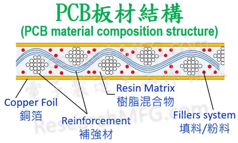
Substrate Layer
The substrate layer is the foundation of a PCB, providing a stable base for the other layers. The most common substrate materials used in PCB manufacturing are:
-
FR-4: A flame-retardant, fiberglass-reinforced epoxy laminate, FR-4 is the most widely used substrate material due to its excellent mechanical and electrical properties.
-
Polyimide: This high-performance polymer offers superior thermal resistance and flexibility, making it ideal for applications requiring high reliability and durability.
-
Ceramic: Ceramic substrates, such as alumina or beryllium oxide, are used in high-frequency and high-power applications due to their excellent thermal conductivity and low dielectric loss.
Copper Layer
The copper layer is responsible for carrying electrical signals between components on the PCB. This layer is typically made of a thin sheet of copper foil, which is laminated onto the substrate using heat and pressure. The thickness of the copper layer can vary depending on the application, with common thicknesses ranging from 0.5 oz to 2 oz per square foot.
Solder Mask Layer
The solder mask layer is a protective coating applied over the copper layer, leaving only the exposed areas where components will be soldered. This layer serves several purposes:
-
Insulation: The solder mask prevents accidental short circuits by insulating the copper traces.
-
Protection: It protects the copper layer from oxidation and corrosion, increasing the longevity of the PCB.
-
Aesthetics: Solder masks are available in various colors, allowing for improved visual appeal and readability of the PCB.
Silkscreen Layer
The silkscreen layer is the final layer applied to a PCB, consisting of text, symbols, and logos printed onto the solder mask. This layer helps with the identification of components, connectors, and other features on the board. Silkscreen is typically printed in white, but other colors are available for improved contrast or aesthetics.
Common Materials Used in PCB Composition
In addition to the layers mentioned above, PCBs incorporate various other materials to ensure optimal performance and reliability. Some of these materials include:
Copper Plating
Copper plating is used to create the conductive traces, pads, and vias on a PCB. There are two primary methods for copper plating:
-
Electroless plating: This process involves depositing a thin layer of copper onto the substrate through a chemical reaction, without the use of an external electrical current.
-
Electrolytic plating: In this process, an electrical current is used to deposit a thicker layer of copper onto the substrate, providing better conductivity and durability.
Solder
Solder is an alloy used to create electrical and mechanical connections between components and the PCB. The most common types of solder used in PCB assembly are:
-
Lead-based solder: Traditionally, a tin-lead alloy (SnPb) was used due to its low melting point and excellent wetting properties. However, due to environmental and health concerns, lead-based solder is being phased out in favor of lead-free alternatives.
-
Lead-free solder: Lead-free solder alloys, such as SAC (tin-silver-copper) and SN100C (tin-copper-nickel-germanium), have become the standard in PCB assembly. These alloys offer similar performance to lead-based solder while being more environmentally friendly.
Surface Finishes
Surface finishes are applied to the exposed copper areas of a PCB to protect them from oxidation and enhance solderability. Some common surface finishes include:
-
HASL (Hot Air Solder Leveling): A tin-lead or lead-free solder alloy is applied to the copper surfaces, creating a thin, uniform layer that protects the copper and improves solderability.
-
ENIG (Electroless Nickel Immersion Gold): A layer of nickel is deposited onto the copper, followed by a thin layer of gold. ENIG provides excellent durability, solderability, and shelf life.
-
OSP (Organic Solderability Preservative): A thin, transparent organic coating is applied to the copper surfaces, protecting them from oxidation and ensuring good solderability.

PCB Composition and Manufacturing Process
The composition of a PCB is closely tied to its manufacturing process. Understanding the steps involved in PCB fabrication can provide valuable insights into the materials and layers that make up these boards.
PCB Design
The first step in PCB manufacturing is the design phase, where the schematic and layout of the board are created using specialized software. During this phase, designers determine the number of layers, component placement, and routing of the conductive traces.
PCB Fabrication
Once the design is finalized, the PCB fabrication process begins. The main steps involved in PCB fabrication are:
-
Substrate preparation: The substrate material is cut to size and cleaned to remove any contaminants.
-
Copper lamination: Copper foil is laminated onto the substrate using heat and pressure.
-
Photoresist application: A light-sensitive polymer, called photoresist, is applied to the copper layer.
-
Exposure and development: The photoresist is exposed to UV light through a patterned mask, and then developed to remove the unexposed areas.
-
Etching: The exposed copper is etched away using a chemical solution, leaving only the desired conductive traces and pads.
-
Solder mask application: The solder mask is applied and cured, protecting the copper traces and insulating the board.
-
Silkscreen printing: The silkscreen layer is printed onto the solder mask, providing text and symbols for component identification.
-
Surface finish application: The desired surface finish is applied to the exposed copper areas to protect them and enhance solderability.
PCB Assembly
After the PCB fabrication process is complete, the board moves on to the assembly phase. During assembly, components are placed and soldered onto the board, creating a functional electronic device.

Environmental Considerations in PCB Composition
As environmental concerns continue to grow, the electronics industry has been working towards more eco-friendly PCB materials and manufacturing processes.
Halogen-Free PCBs
Halogenated flame retardants, such as brominated and chlorinated compounds, have been widely used in PCB substrates to improve fire resistance. However, these substances can release toxic fumes when exposed to high temperatures, posing health and environmental risks. As a result, halogen-free PCB materials, such as halogen-free FR-4 and polyimide, have gained popularity in recent years.
Lead-Free Solder
The transition from lead-based to lead-free solder has been a significant step towards more environmentally friendly PCB composition. Lead-free solder alloys, such as SAC and SN100C, have become the standard in PCB assembly, reducing the environmental impact of electronic waste.
Recyclable Materials
The use of recyclable materials in PCB composition is another way to minimize environmental impact. Some manufacturers have begun using recycled copper and other metals in their PCB production, reducing the demand for virgin raw materials.

Future Trends in PCB Composition
As technology continues to advance, the composition of PCBs is likely to evolve to meet new challenges and demands. Some emerging trends in PCB composition include:
High-Frequency Materials
With the growing demand for high-speed and high-frequency applications, such as 5G networks and automotive radar systems, the development of new PCB substrate materials has become increasingly important. Materials like Rogers RO4000 series and PTFE (polytetrafluoroethylene) offer excellent high-frequency performance, low dielectric loss, and thermal stability.
Flexible and Stretchable PCBs
Flexible and stretchable PCBs are gaining traction in wearable electronics, medical devices, and other applications requiring conformable and durable circuits. These PCBs are typically made using flexible substrate materials, such as polyimide or PET (polyethylene terephthalate), and stretchable conductive inks or polymers.
Embedded Components
Embedded component technology involves integrating passive components, such as resistors and capacitors, directly into the PCB substrate. This approach can reduce the size and weight of the PCB, improve signal integrity, and enhance overall system performance. As this technology matures, it is likely to become more prevalent in PCB composition.
Frequently Asked Questions (FAQ)
-
What is the most common substrate material used in PCBs?
FR-4, a fiberglass-reinforced epoxy laminate, is the most widely used substrate material in PCB manufacturing due to its excellent mechanical and electrical properties. -
What is the purpose of the solder mask layer in a PCB?
The solder mask layer serves as a protective coating, insulating the copper traces, preventing short circuits, and protecting the copper from oxidation and corrosion. It also provides improved aesthetics and readability of the PCB. -
What are the differences between lead-based and lead-free solder?
Lead-based solder, typically a tin-lead alloy, has been traditionally used in PCB assembly due to its low melting point and excellent wetting properties. However, due to environmental and health concerns, lead-free solder alloys, such as SAC and SN100C, have become the standard in recent years. Lead-free solder offers similar performance while being more environmentally friendly. -
What are the main steps involved in PCB fabrication?
The main steps in PCB fabrication include substrate preparation, copper lamination, photoresist application, exposure and development, etching, solder mask application, silkscreen printing, and surface finish application. -
What are some emerging trends in PCB composition?
Some emerging trends in PCB composition include the use of high-frequency materials for 5G networks and automotive radar systems, flexible and stretchable PCBs for wearable electronics and medical devices, and embedded component technology for reduced size and weight, improved signal integrity, and enhanced system performance.
Conclusion
PCBs are complex assemblies of various materials, each serving a critical role in the overall performance and reliability of electronic devices. Understanding the composition of PCBs, from the substrate and copper layers to the solder mask and surface finishes, is essential for designers, manufacturers, and end-users alike.
As technology continues to advance and environmental concerns grow, the composition of PCBs is likely to evolve, incorporating new materials and manufacturing processes to meet the demands of the future. By staying informed about the latest developments in PCB composition, we can ensure that our electronic devices remain at the forefront of innovation while minimizing their environmental impact.
| Layer | Material | Purpose |
|---|---|---|
| Substrate | FR-4, Polyimide, Ceramic | Provides a stable base for other layers |
| Copper | Copper foil | Carries electrical signals between components |
| Solder Mask | Polymer coating | Insulates copper traces, protects from oxidation, improves aesthetics |
| Silkscreen | Ink (white or other colors) | Provides text and symbols for component identification |
| Material | Application |
|---|---|
| Copper plating | Creates conductive traces, pads, and vias |
| Solder | Creates electrical and mechanical connections |
| Surface finishes | Protects exposed copper, enhances solderability |
By understanding the composition of PCBs and the materials used in their manufacturing, we can better appreciate the complexity and importance of these essential components in our daily lives.


Leave a Reply