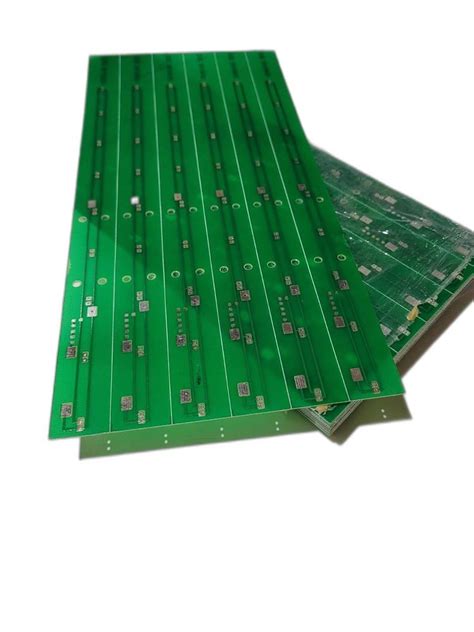
Introduction to PCB Fabrication
PCB fabrication is the process of manufacturing printed circuit boards used in electronic devices. It involves several steps to transform a PCB design into a physical board ready for component assembly. Setting up a PCB fabrication facility requires careful planning, appropriate equipment selection, and adherence to industry standards and best practices.
Key Aspects of PCB Fabrication Set-Up
- Facility Layout and Cleanroom Environment
- Equipment Selection and Maintenance
- Material Sourcing and Inventory Management
- Quality Control and Testing Procedures
- Staff Training and Safety Measures
Facility Layout and Cleanroom Environment
Importance of Proper Facility Layout
A well-designed PCB fabrication facility layout ensures efficient workflow, minimizes contamination risks, and promotes a safe working environment. Key considerations include:
- Separating cleanroom areas from other production zones
- Optimizing material flow and minimizing cross-contamination risks
- Providing adequate space for equipment, storage, and personnel movement
Cleanroom Standards and Classifications
Cleanrooms are essential for PCB fabrication to prevent particulate contamination. The International Organization for Standardization (ISO) defines cleanroom classifications based on the allowable concentration of airborne particles.
| ISO Class | Maximum Particles/m³ (≥0.5 µm) | Example Applications |
|---|---|---|
| ISO 1 | 10 | Microelectronics |
| ISO 2 | 100 | Semiconductor |
| ISO 3 | 1,000 | Precision optics |
| ISO 4 | 10,000 | PCB fabrication |
| ISO 5 | 100,000 | General manufacturing |
Implementing proper filtration systems, air showers, and gowning procedures helps maintain the required cleanroom standards.

Equipment Selection and Maintenance
Essential PCB Fabrication Equipment
Investing in high-quality equipment is crucial for consistent PCB production. Key equipment includes:
- Photoplotter for film generation
- Exposure units for photoresist patterning
- Etching machines for copper removal
- Drill machines for hole drilling
- Automated optical inspection (AOI) systems for quality control
Equipment Maintenance and Calibration
Regular maintenance and calibration of PCB fabrication equipment ensure optimal performance and minimize downtime. Establish a preventive maintenance schedule that includes:
- Cleaning and lubrication of moving parts
- Replacing consumables (e.g., drill bits, filters)
- Calibrating critical parameters (e.g., exposure time, etching rates)
- Conducting periodic equipment audits and performance tests

Material Sourcing and Inventory Management
Selecting High-Quality Materials
Using high-quality materials is essential for producing reliable PCBs. Key materials include:
- Copper-clad laminates (e.g., FR-4, polyimide)
- Photoresists and developers
- Etching chemicals (e.g., ferric chloride, ammonium persulfate)
- Solder mask and silkscreen inks
Establish relationships with reputable suppliers and conduct incoming material inspections to ensure consistency and compliance with specifications.
Inventory Management Practices
Effective inventory management helps minimize material waste, reduces storage costs, and ensures timely availability of components. Implement practices such as:
- Just-in-time (JIT) inventory management
- First-in, first-out (FIFO) material usage
- Regularly updating inventory records and conducting physical counts
- Monitoring supplier lead times and adjusting reorder points accordingly

Quality Control and Testing Procedures
In-Process Quality Control
Implementing in-process quality control measures helps identify and address issues early in the fabrication process. Key steps include:
- Conducting visual inspections after each critical process step
- Monitoring process parameters (e.g., exposure time, etching rates)
- Utilizing statistical process control (SPC) techniques to detect process deviations
Final Inspection and Testing
Final inspection and testing ensure that PCBs meet customer specifications and performance requirements. Common techniques include:
- Automated optical inspection (AOI) for identifying surface defects
- Electrical testing (e.g., continuity, insulation resistance)
- Microsectioning for analyzing internal structures
- Functional testing under various environmental conditions
Establish clear acceptance criteria and maintain detailed inspection and test records for traceability purposes.
Staff Training and Safety Measures
Employee Training Programs
Investing in employee training is crucial for maintaining a skilled and knowledgeable workforce. Develop training programs that cover:
- PCB fabrication process fundamentals
- Equipment operation and maintenance procedures
- Quality control and testing techniques
- Cleanroom protocols and contamination control
Regularly assess employee competency and provide ongoing training to keep skills up-to-date.
Workplace Safety and Health
Prioritizing workplace safety and health is essential for protecting employees and ensuring compliance with regulations. Key measures include:
- Providing personal protective equipment (PPE) such as gloves, goggles, and respirators
- Implementing proper ventilation and exhaust systems for hazardous chemicals
- Conducting regular safety training and emergency response drills
- Maintaining up-to-date safety data sheets (SDS) for all chemicals used in the facility
Frequently Asked Questions (FAQ)
1. What is the typical lead time for PCB fabrication?
Lead times for PCB fabrication vary depending on the complexity of the design, material availability, and production capacity. Typical lead times range from 1-2 weeks for standard designs to 4-6 weeks for more complex or custom boards.
2. How do I select the right copper thickness for my PCB?
The choice of copper thickness depends on factors such as current carrying requirements, signal integrity, and manufacturing constraints. Common copper thicknesses include 0.5 oz (17 µm), 1 oz (35 µm), and 2 oz (70 µm). Consult with your PCB fabricator to determine the optimal copper thickness for your application.
3. What is the minimum feature size achievable in PCB fabrication?
The minimum feature size depends on the fabrication process and equipment capabilities. Typical minimum feature sizes range from 3-4 mils (75-100 µm) for standard processes to 1-2 mils (25-50 µm) for advanced processes. Always verify the capabilities of your PCB fabricator before finalizing your design.
4. How can I ensure the reliability of my PCBs?
To ensure PCB reliability, consider the following:
- Use high-quality materials and components
- Follow design guidelines for manufacturability and signal integrity
- Implement robust quality control and testing procedures
- Conduct accelerated life testing and failure analysis to identify potential weaknesses
5. What environmental regulations should I be aware of for PCB fabrication?
PCB fabrication involves the use of hazardous chemicals and generates waste that must be properly managed. Key environmental regulations include:
- Restriction of Hazardous Substances (RoHS) directive
- Waste Electrical and Electronic Equipment (WEEE) directive
- Registration, Evaluation, Authorization, and Restriction of Chemicals (REACH) regulation
Ensure compliance with local and international environmental regulations to avoid penalties and maintain a sustainable operation.
Conclusion
Setting up a PCB fabrication facility requires careful planning, investment in equipment and infrastructure, and adherence to industry standards and best practices. By focusing on facility layout, equipment maintenance, material sourcing, quality control, and employee training, you can establish a reliable and efficient PCB fabrication operation. Continuously monitor and improve your processes to stay competitive in the ever-evolving electronics industry.


Leave a Reply