Introduction to PCB Production
Printed Circuit Board (PCB) production is a complex process that involves multiple steps and technologies. PCBs are essential components in almost all electronic devices, from smartphones and computers to medical equipment and aerospace systems. In this article, we will explore the various aspects of PCB production, including the materials used, the manufacturing process, quality control, and more.
What is a PCB?
A PCB is a flat board made of insulating materials, such as fiberglass or plastic, with conductive copper traces etched onto its surface. These traces connect various electronic components, such as resistors, capacitors, and integrated circuits (ICs), to form a functional electronic circuit. PCBs come in different sizes, shapes, and layer counts, depending on the complexity of the circuit and the application requirements.
Why are PCBs important?
PCBs have revolutionized the electronics industry by providing a reliable and efficient way to interconnect electronic components. They offer several advantages over traditional point-to-point wiring, such as:
- Reduced size and weight
- Improved reliability and durability
- Increased circuit density and complexity
- Easier assembly and maintenance
- Lower manufacturing costs
PCB Materials
The choice of materials used in PCB production depends on the specific application requirements, such as the operating environment, electrical performance, and cost. The most common materials used in PCB production are:
Substrate Materials
The substrate is the base material of the PCB, providing mechanical support and electrical insulation. The most common substrate materials are:
- FR-4: A glass-reinforced epoxy laminate, widely used for general-purpose PCBs.
- High-Tg FR-4: A variant of FR-4 with improved thermal stability, suitable for high-temperature applications.
- Polyimide: A high-performance polymer with excellent thermal and chemical resistance, used in aerospace and military applications.
- PTFE (Teflon): A low-loss, high-frequency material used in RF and microwave applications.
Copper Foil
Copper foil is the conductive material used to create the circuit traces on the PCB. It is typically available in thicknesses ranging from 0.5 oz to 2 oz per square foot (17 to 68 μm). The choice of copper thickness depends on the current-carrying requirements and the desired trace width and spacing.
Solder Mask
Solder mask is a thin, protective layer applied over the copper traces to prevent accidental short circuits and improve the PCB’s appearance. It is typically green in color but can also be found in other colors, such as blue, red, or black. Solder mask also provides a surface for silk-screen printing of component labels and other markings.
Surface Finish
The surface finish is a coating applied to the exposed copper areas of the PCB to prevent oxidation and improve solderability. The most common surface finishes are:
- HASL (Hot Air Solder Leveling): A tin-lead alloy coating applied by dipping the PCB in molten solder and leveling the surface with hot air.
- ENIG (Electroless Nickel Immersion Gold): A two-layer coating consisting of a nickel underlayer and a thin gold toplayer, providing excellent solderability and shelf life.
- OSP (Organic Solderability Preservative): A thin, organic coating that protects the copper surface from oxidation and enhances solderability.
PCB Manufacturing Process
The PCB manufacturing process involves several steps, each requiring specialized equipment and skilled operators. The main steps in PCB production are:
Design and Layout
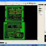
The first step in PCB production is to create a design and layout of the circuit using specialized software, such as Altium Designer or Eagle. The design includes the schematic diagram, which shows the electrical connections between components, and the layout, which specifies the physical placement of components and routing of traces on the PCB.
PCB Fabrication
Once the design is finalized, the PCB fabrication process begins. The main steps in PCB fabrication are:
-
Copper Clad Laminate Preparation: The substrate material is cut to size and cleaned to remove any contaminants.
-
Drilling: Holes are drilled into the substrate to accommodate through-hole components and vias (interconnects between layers).
-
Patterning: The copper foil is patterned using a photolithography process. A photoresist layer is applied to the copper, exposed to UV light through a photomask, and developed to create the desired trace pattern.
-
Etching: The exposed copper is etched away using a chemical solution, leaving only the desired traces.
-
Lamination: For multi-layer PCBs, the patterned layers are aligned and bonded together under high pressure and temperature.
-
Solder Mask Application: The solder mask is applied to the PCB surface and cured using UV light.
-
Surface Finish Application: The desired surface finish is applied to the exposed copper areas.
-
Silk-Screen Printing: Component labels and other markings are printed onto the solder mask using a silk-screen process.
-
Electrical Testing: The PCB is tested for continuity, shorts, and opens using automated test equipment (ATE).
PCB Assembly
After the PCB fabrication is complete, the electronic components are assembled onto the board. The main steps in PCB assembly are:
-
Solder Paste Application: Solder paste, a mixture of tiny solder particles and flux, is applied to the pads on the PCB using a stencil or screen-printing process.
-
Component Placement: The components are placed onto the PCB using automated pick-and-place machines or manual placement for low-volume or complex assemblies.
-
Reflow Soldering: The PCB is heated in a reflow oven, causing the solder paste to melt and form a permanent bond between the components and the PCB.
-
Inspection: The assembled PCB is visually inspected for defects, such as misaligned components, solder bridges, or insufficient solder joints.
-
Functional Testing: The assembled PCB is tested for proper functionality using various test methods, such as in-circuit testing (ICT), boundary scan, or functional testing.

Quality Control in PCB Production
Quality control is a critical aspect of PCB production, ensuring that the finished product meets the required specifications and performance standards. Some of the key quality control measures in PCB production include:
Incoming Material Inspection
All incoming materials, such as substrate, copper foil, and components, are inspected for quality and conformance to specifications before being used in production.
In-Process Inspection
During the PCB fabrication and assembly processes, various in-process inspections are performed to detect and correct any defects or deviations from the specified parameters. These inspections may include:
- Visual inspection for defects, such as scratches, dents, or discoloration
- Automated optical inspection (AOI) for detecting solder defects, component placement errors, or missing components
- X-ray inspection for detecting internal defects, such as voids or cracks in solder joints
- Electrical testing for continuity, shorts, and opens
Final Inspection
After the PCB assembly is complete, a final inspection is performed to ensure that the finished product meets all the required specifications and quality standards. This may include:
- Visual inspection for cosmetic defects, such as scratches, dents, or discoloration
- Functional testing to verify that the PCB performs as intended under various operating conditions
- Burn-in testing to identify early failures and improve reliability
- Environmental testing to ensure that the PCB can withstand the specified temperature, humidity, and vibration levels
Advanced Topics in PCB Production
High-Density Interconnect (HDI) PCBs
HDI PCBs are a type of PCB that features high-density routing and fine-pitch components to achieve smaller size and higher performance. HDI PCBs use advanced fabrication techniques, such as microvias, buried vias, and sequential lamination, to create complex multi-layer structures with reduced layer count and improved signal integrity.
Flexible and Rigid-Flex PCBs
Flexible PCBs are made using thin, flexible substrate materials, such as polyimide or polyester, to allow for bending and folding of the circuit. Rigid-flex PCBs combine rigid and flexible sections in a single board, providing the benefits of both types of PCBs in a compact and reliable package. Flexible and rigid-flex PCBs are commonly used in wearable devices, medical equipment, and aerospace applications.
Embedded Components
Embedded components are a relatively new technology in PCB production that involves embedding passive components, such as resistors and capacitors, inside the PCB substrate. This technique offers several advantages, such as reduced board size, improved electrical performance, and increased reliability. However, it also requires specialized design and fabrication processes and may not be suitable for all applications.
Frequently Asked Questions (FAQ)
-
What is the difference between a single-sided and a double-sided PCB?
A single-sided PCB has conductive traces on only one side of the substrate, while a double-sided PCB has traces on both sides. Double-sided PCBs offer higher circuit density and more design flexibility but are more complex and expensive to manufacture. -
What is the purpose of vias in a PCB?
Vias are conductive holes drilled through the PCB substrate to interconnect traces on different layers. They allow for more compact routing and improved signal integrity in multi-layer PCBs. -
What is the difference between through-hole and surface-mount components?
Through-hole components have long leads that are inserted into holes drilled in the PCB and soldered on the opposite side. Surface-mount components have small pins or pads that are soldered directly onto the surface of the PCB. Surface-mount components are smaller and more suitable for high-density designs, while through-hole components are more robust and easier to assemble manually. -
What is the purpose of a solder mask on a PCB?
A solder mask is a thin, protective layer applied over the copper traces on a PCB to prevent accidental short circuits and improve the appearance of the board. It also provides a surface for silk-screen printing of component labels and other markings. -
What is the typical turnaround time for PCB production?
The turnaround time for PCB production depends on various factors, such as the complexity of the design, the fabrication and assembly processes required, and the manufacturer’s workload. Typical turnaround times range from a few days for simple, quick-turn PCBs to several weeks for complex, high-reliability PCBs.
Conclusion
PCB production is a complex and multi-faceted process that involves various materials, technologies, and quality control measures. Understanding the basics of PCB production is essential for anyone involved in electronics design, manufacturing, or procurement. By familiarizing yourself with the materials, processes, and advanced topics covered in this article, you can make informed decisions and ensure the success of your PCB projects.
As the electronics industry continues to evolve, PCB production technologies will also advance to meet the growing demands for smaller, faster, and more reliable electronic devices. Keeping up with these advancements and adopting best practices in PCB design and manufacturing will be key to staying competitive in this dynamic field.
Leave a Reply