Introduction to PCBA Testing
Printed Circuit Board Assembly (PCBA) is a crucial process in the manufacturing of electronic devices. To ensure the quality and reliability of the final product, various PCBA test and inspection methods are employed throughout the assembly process. These methods help identify defects, ensure proper functionality, and maintain the overall quality of the PCBAs.
In this article, we will explore several PCBA test and inspection methods, their importance, and how they contribute to the manufacturing of high-quality electronic products.
Why is PCBA Testing Important?
PCBA testing is essential for several reasons:
-
Quality Assurance: Testing helps ensure that the assembled PCBs meet the required quality standards and specifications.
-
Defect Detection: Various testing methods help identify defects such as short circuits, open circuits, incorrect component placement, and soldering issues.
-
Functionality Verification: Testing verifies that the assembled PCBs function as intended and meet the desired performance criteria.
-
Cost Reduction: Early detection of defects during the assembly process reduces the cost of rework and prevents faulty products from reaching the market.
-
Reliability Enhancement: Thorough testing helps improve the overall reliability of the electronic devices, minimizing the risk of failures and customer complaints.
Types of PCBA Test and Inspection Methods
There are several PCBA test and inspection methods used in the industry. Let’s explore some of the most common methods:
1. Visual Inspection
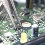
Visual inspection is the most basic and widely used method for PCBA testing. It involves the use of human eyes or automated optical inspection (AOI) systems to visually examine the assembled PCBs for defects. Visual inspection checks for the following:
- Component placement accuracy
- Soldering quality
- Proper component orientation
- Presence of foreign objects or debris
- PCB surface cleanliness
Visual inspection can be performed at various stages of the assembly process, such as pre-reflow, post-reflow, and final inspection.
2. Automated Optical Inspection (AOI)
Automated Optical Inspection (AOI) is an advanced form of visual inspection that uses high-resolution cameras and image processing software to detect defects on the assembled PCBs. AOI systems compare the captured images of the PCBs with pre-defined reference images to identify anomalies.
AOI is capable of detecting the following defects:
- Missing or misaligned components
- Solder bridging or insufficiency
- Incorrect component polarity
- Lifted or tombstoned components
- Solder paste defects
AOI is a fast and efficient method for inspecting large volumes of PCBs, making it suitable for high-volume production.
3. In-Circuit Testing (ICT)
In-Circuit Testing (ICT) is a comprehensive testing method that verifies the functionality and connectivity of individual components on the assembled PCBs. ICT uses a bed-of-nails fixture, which consists of a matrix of spring-loaded pins that make contact with specific test points on the PCB.
ICT performs the following tests:
- Continuity testing
- Resistance measurement
- Capacitance measurement
- Diode and transistor testing
- Inductance measurement
- Voltage measurement
ICT is highly effective in detecting manufacturing defects and ensuring the proper functioning of individual components. However, it requires the design of a custom test fixture for each PCB, which can be time-consuming and costly.
4. Flying Probe Testing
Flying Probe Testing is an alternative to ICT that eliminates the need for a custom test fixture. Instead, it uses a set of programmable probes that move across the PCB surface to make contact with the test points. Flying Probe Testing offers flexibility and adaptability, as the test program can be easily modified for different PCB designs.
Flying Probe Testing performs similar tests to ICT, including:
- Continuity testing
- Resistance measurement
- Capacitance measurement
- Diode and transistor testing
Flying Probe Testing is suitable for low-volume production or prototype testing, where the cost of developing a custom ICT fixture may not be justified.
5. Functional Testing
Functional Testing is a method that verifies the overall functionality and performance of the assembled PCBs. It involves applying input signals to the PCB and measuring the output signals to ensure they meet the desired specifications. Functional Testing can be performed using specialized test equipment or by integrating the PCB into the final product.
Functional Testing checks for the following:
- Input/output functionality
- Signal integrity
- Power consumption
- Timing and synchronization
- Communication protocols
Functional Testing is crucial for ensuring that the assembled PCBs operate as intended and meet the required performance criteria.
6. Boundary Scan Testing
Boundary Scan Testing, also known as JTAG (Joint Test Action Group) testing, is a method that utilizes the built-in test circuitry of integrated circuits (ICs) to test the interconnections between them. It involves accessing the boundary-scan cells of the ICs through a standard interface and running test patterns to verify the connectivity and functionality of the ICs.
Boundary Scan Testing is particularly useful for testing complex PCBs with high-density interconnects and ball grid array (BGA) packages. It can detect the following defects:
- Open circuits
- Short circuits
- Stuck-at faults
- Interconnect defects
Boundary Scan Testing requires the ICs to have built-in boundary-scan capabilities and the PCB design to include the necessary test access points.
7. X-Ray Inspection
X-Ray Inspection is a non-destructive testing method that uses X-rays to examine the internal structure of the assembled PCBs. It is particularly useful for inspecting solder joints and connections that are not visible from the surface, such as those under BGA packages or through-hole components.
X-Ray Inspection can detect the following defects:
- Solder voids
- Solder bridging
- Insufficient solder
- Component placement issues
- Internal cracks or damage
X-Ray Inspection provides detailed images of the internal structure of the PCBs, allowing for accurate analysis and defect detection.

Comparison of PCBA Test and Inspection Methods
| Method | Advantages | Disadvantages |
|---|---|---|
| Visual Inspection | – Simple and cost-effective – Can detect surface defects |
– Subjective and prone to human error – Limited to surface defects |
| Automated Optical Inspection (AOI) | – Fast and efficient – Suitable for high-volume production – Detects surface defects accurately |
– Limited to surface defects – Requires programming and setup |
| In-Circuit Testing (ICT) | – Comprehensive testing of individual components – Detects manufacturing defects effectively |
– Requires custom test fixtures – Time-consuming and costly setup |
| Flying Probe Testing | – Flexible and adaptable – No custom fixtures required |
– Slower than ICT – Limited test coverage compared to ICT |
| Functional Testing | – Verifies overall functionality and performance – Ensures product meets specifications |
– Requires specialized test equipment or integration into the final product |
| Boundary Scan Testing | – Useful for testing complex PCBs with high-density interconnects – Detects interconnect defects |
– Requires ICs with built-in boundary-scan capabilities – Limited to testing interconnections between ICs |
| X-Ray Inspection | – Non-destructive testing of internal structure – Detects defects not visible from the surface |
– Expensive equipment – Requires skilled operators for interpretation |
Best Practices for PCBA Testing
To ensure effective and efficient PCBA testing, consider the following best practices:
-
Develop a Comprehensive Test Strategy: Define a test strategy that covers all critical aspects of the PCBA, including component functionality, interconnections, and overall performance.
-
Implement a Multi-Stage Testing Approach: Perform testing at various stages of the assembly process, such as pre-reflow, post-reflow, and final inspection, to catch defects early and reduce rework costs.
-
Choose the Right Test Methods: Select the appropriate test methods based on the complexity of the PCBs, production volume, and available resources. Consider a combination of methods to achieve comprehensive test coverage.
-
Establish Clear Acceptance Criteria: Define clear acceptance criteria for each test method, specifying the allowable defect types, sizes, and quantities. Ensure that all stakeholders agree on the criteria.
-
Maintain Proper Documentation: Document the test procedures, acceptance criteria, and test results for traceability and future reference. Use a centralized database or quality management system to store and manage the documentation.
-
Regularly Calibrate and Maintain Test Equipment: Ensure that all test equipment is regularly calibrated and maintained to ensure accurate and reliable test results.
-
Provide Training to Operators: Train the operators on the proper use of test equipment, interpretation of test results, and identification of defects. Regularly update their skills and knowledge to keep up with advancements in testing technologies.
-
Analyze Test Data for Continuous Improvement: Collect and analyze test data to identify recurring defects, process bottlenecks, and areas for improvement. Use the insights gained to optimize the assembly process and enhance overall quality.
FAQ
-
Q: What is the difference between ICT and Flying Probe Testing?
A: ICT requires a custom bed-of-nails test fixture specific to each PCB design, while Flying Probe Testing uses programmable probes that move across the PCB surface. ICT is faster and provides comprehensive testing, while Flying Probe Testing offers flexibility and adaptability without the need for custom fixtures. -
Q: Can AOI detect defects that are not visible from the surface?
A: No, AOI is limited to detecting surface defects. For detecting defects that are not visible from the surface, such as those under BGA packages or through-hole components, X-Ray Inspection is used. -
Q: Is Functional Testing sufficient for ensuring the quality of PCBAs?
A: While Functional Testing is crucial for verifying the overall functionality and performance of PCBAs, it should be used in combination with other test methods to ensure comprehensive defect detection and quality assurance. -
Q: How often should test equipment be calibrated?
A: The calibration frequency depends on the specific equipment and the manufacturer’s recommendations. Generally, test equipment should be calibrated at least annually or more frequently if specified by the manufacturer or required by industry standards. -
Q: What are the benefits of implementing a multi-stage testing approach?
A: Implementing a multi-stage testing approach helps catch defects early in the assembly process, reduces rework costs, and ensures that defects are not carried forward to subsequent stages. It allows for prompt identification and correction of issues, improving overall quality and efficiency.
Conclusion
PCBA test and inspection methods play a vital role in ensuring the quality, reliability, and functionality of assembled PCBs. From visual inspection to advanced techniques like AOI, ICT, Flying Probe Testing, Functional Testing, Boundary Scan Testing, and X-Ray Inspection, each method contributes to detecting defects and verifying the integrity of the PCBAs.
By implementing a comprehensive test strategy, choosing the right test methods, establishing clear acceptance criteria, and following best practices, manufacturers can effectively identify and address defects, reduce rework costs, and deliver high-quality electronic products to their customers.
As technology advances and PCBAs become more complex, it is essential to stay updated with the latest testing technologies and techniques. Continuous improvement and adaptation of testing methods will be key to meeting the ever-increasing quality demands of the electronics industry.

Leave a Reply