Understanding Single Layer PCBs and Their Production
Single layer PCBs, also known as single-sided PCBs, are printed circuit boards that have conductive traces and components on only one side of the board. These PCBs are widely used in various electronic devices and applications due to their simplicity, cost-effectiveness, and ease of manufacturing. In this article, we will delve into the world of single layer PCB Production, exploring the materials, processes, and best practices involved in creating these essential components.
What Are Single Layer PCBs?
Single layer PCBs are the most basic type of printed circuit board, consisting of a single layer of conductive copper traces and components on one side of an insulating substrate material, typically FR-4 (a glass-reinforced epoxy laminate). The other side of the board is left bare, without any conductive traces or components.
Advantages of Single Layer PCBs
- Cost-effective: Single layer PCBs are generally less expensive to produce compared to multi-layer PCBs due to their simpler design and fewer manufacturing steps.
- Easy to design and manufacture: The single-sided nature of these PCBs makes them easier to design and manufacture, reducing the overall complexity of the production process.
- Suitable for low-complexity circuits: Single layer PCBs are ideal for simple electronic circuits with fewer components and connections, such as those found in LED lighting, power supplies, and basic sensors.
Materials Used in Single Layer PCB Production
The primary materials used in the production of single layer PCBs include:
-
Substrate: The most common substrate material for single layer PCBs is FR-4, a glass-reinforced epoxy laminate that offers excellent electrical insulation, mechanical strength, and thermal stability.
-
Copper foil: A thin layer of copper foil, typically 1 oz (35 µm) or 2 oz (70 µm) in thickness, is laminated onto the FR-4 substrate to create the conductive traces and pads for components.
-
Solder mask: A protective layer of polymer is applied over the copper traces, leaving only the exposed pads for soldering components. The solder mask helps prevent short circuits and provides a barrier against environmental factors.
-
Silkscreen: A layer of ink is printed on the PCB surface to display text, logos, and component outlines, aiding in the assembly and identification of the board.
Single Layer PCB Production Process
The production of single layer PCBs involves several key steps, each playing a crucial role in ensuring the quality and functionality of the final product.
1. PCB Design and Layout
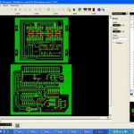
The first step in single layer PCB production is designing the circuit schematic and creating the PCB layout using specialized software tools such as Altium Designer, Eagle, or KiCad. The layout determines the placement of components, routing of traces, and the overall dimensions of the board.
2. Substrate Preparation
The FR-4 substrate is cut to the desired size and shape, and the copper foil is laminated onto one side of the substrate using heat and pressure. This process ensures a strong bond between the copper and the substrate, creating a stable foundation for the subsequent steps.
3. Drilling
Holes are drilled through the PCB at the locations specified in the design files. These holes serve as mounting points for through-hole components and provide electrical connections between the top and bottom layers of the board (in the case of double-sided PCBs).
4. Copper Etching
The PCB undergoes a photolithography process, where a photoresist layer is applied to the copper surface and exposed to UV light through a photomask containing the desired trace patterns. The unexposed areas of the photoresist are then removed, exposing the underlying copper. The board is then subjected to a chemical etching process, which removes the unwanted copper, leaving only the desired traces and pads.
5. Solder Mask Application
A layer of solder mask is applied to the PCB surface, covering the copper traces while leaving the component pads exposed. The solder mask is typically green in color but can be customized to other colors as well. This layer protects the traces from oxidation and prevents accidental short circuits during the soldering process.
6. Silkscreen Printing
The silkscreen layer is printed onto the solder mask using ink, displaying text, logos, and component outlines. This layer aids in the assembly process and helps identify the various components and their locations on the board.
7. Surface Finishing
To enhance the solderability and protect the exposed copper pads, a surface finish is applied to the PCB. Common surface finishes for single layer PCBs include:
- Hot Air Solder Leveling (HASL): A layer of solder is applied to the pads and then leveled using hot air, creating a flat, solderable surface.
- Electroless Nickel Immersion Gold (ENIG): A layer of nickel is deposited onto the copper pads, followed by a thin layer of gold, providing excellent solderability and corrosion resistance.
- Organic Solderability Preservative (OSP): A thin, organic coating is applied to the copper pads, protecting them from oxidation and ensuring good solderability.
8. Electrical Testing
Before the PCBs are shipped to the customer, they undergo rigorous electrical testing to ensure that all the connections are properly made and that there are no short circuits or open connections. This step is critical in guaranteeing the functionality and reliability of the final product.
Best Practices for Single Layer PCB Production
To ensure the highest quality and reliability of single layer PCBs, manufacturers should adhere to the following best practices:
-
Design for Manufacturability (DFM): Collaborate with experienced PCB designers who understand the limitations and guidelines for single layer PCB design, such as minimum trace widths, clearances, and hole sizes.
-
Material selection: Choose high-quality substrate materials, copper foils, and solder masks to ensure the longevity and performance of the PCBs.
-
Controlled manufacturing environment: Maintain a clean and controlled manufacturing environment to minimize the risk of contamination and defects during the production process.
-
Strict quality control: Implement a comprehensive quality control system that includes regular inspections, testing, and documentation to ensure that each PCB meets the required specifications and standards.
-
Continuous improvement: Regularly review and update the production processes and equipment to incorporate the latest technologies and best practices in PCB manufacturing.

FAQs
1. What is the typical turnaround time for single layer PCB production?
The turnaround time for single layer PCB production can vary depending on the complexity of the design, the quantity ordered, and the manufacturer’s capacity. However, on average, single layer PCBs can be produced within 1-2 weeks from the time the design files are submitted.
2. Can single layer PCBs be used for high-frequency applications?
Single layer PCBs are generally not recommended for high-frequency applications due to their limited ability to control impedance and minimize signal interference. For high-frequency applications, multi-layer PCBs with dedicated power and ground planes are typically used to ensure better signal integrity.
3. What are the minimum feature sizes achievable in single layer PCB production?
The minimum feature sizes for single layer PCBs depend on the capabilities of the manufacturer and the specific production processes used. Typically, the minimum trace width and spacing for single layer PCBs range from 0.15 mm to 0.2 mm (6 to 8 mils), while the minimum hole size is around 0.3 mm (12 mils).
4. How do I choose the right surface finish for my single layer PCBs?
The choice of surface finish depends on factors such as the intended application, environmental conditions, and soldering requirements. HASL is a cost-effective option for general-purpose applications, while ENIG provides superior solderability and corrosion resistance for more demanding environments. OSP is a good choice for applications requiring a flat surface and low cost.
5. Can single layer PCBs be used for prototype and low-volume production?
Yes, single layer PCBs are an excellent choice for prototype and low-volume production due to their low cost, quick turnaround times, and ease of manufacturing. Many PCB manufacturers offer prototype and low-volume services for single layer PCBs, making them accessible to designers and engineers working on new product development.
Conclusion
Single layer PCB production is a critical aspect of the electronics industry, enabling the creation of cost-effective and reliable PCBs for a wide range of applications. By understanding the materials, processes, and best practices involved in single layer PCB production, designers and manufacturers can work together to create high-quality PCBs that meet the demands of modern electronic devices.
As technology continues to evolve, the importance of single layer PCBs in the electronics industry remains strong, offering a simple and affordable solution for many applications. By staying up-to-date with the latest advancements in PCB production and adhering to best practices, manufacturers can ensure the continued success and growth of the single layer PCB market.
| Characteristic | Single Layer PCBs | Multi-Layer PCBs |
|---|---|---|
| Layers | One conductive layer | Two or more conductive layers |
| Cost | Lower cost due to simpler design and fewer manufacturing steps | Higher cost due to increased complexity and additional manufacturing steps |
| Complexity | Suitable for low-complexity circuits with fewer components and connections | Can accommodate high-complexity circuits with dense component placement and intricate routing |
| Applications | LED lighting, power supplies, basic sensors, and other simple electronic devices | High-frequency applications, advanced electronic devices, and complex systems |
| Signal Integrity | Limited ability to control impedance and minimize signal interference | Better signal integrity due to dedicated power and ground planes and controlled impedance |
| Manufacturing Time | Faster turnaround times due to simpler design and fewer production steps | Longer turnaround times due to increased complexity and additional manufacturing steps |
Leave a Reply