What are PCB Design Rules?
PCB design rules are a set of guidelines and best practices used to ensure that a printed circuit board (PCB) is designed and manufactured correctly. These rules cover various aspects of PCB design, including component placement, routing, signal integrity, and manufacturability. By following these rules, designers can create PCBs that are reliable, efficient, and cost-effective.
Why are PCB Design Rules Important?
PCB design rules are essential for several reasons:
-
Ensuring Manufacturability: Following design rules ensures that the PCB can be manufactured using standard processes and equipment, reducing the risk of production delays or failures.
-
Maintaining Signal Integrity: Design rules help maintain signal integrity by specifying proper trace widths, spacing, and routing techniques to minimize crosstalk, reflections, and other signal distortions.
-
Improving Reliability: Adhering to design rules minimizes the risk of PCB failures due to issues such as short circuits, open circuits, or thermal stress.
-
Reducing Costs: By designing a PCB that is easy to manufacture and assemble, designers can reduce production costs and minimize the need for expensive rework or repairs.
Key PCB Design Rules
1. Minimum Trace Width and Spacing
One of the most critical PCB design rules is the minimum trace width and spacing. Trace width refers to the thickness of the copper tracks on the PCB, while spacing refers to the distance between adjacent traces.
The minimum trace width and spacing depend on various factors, such as the PCB’s layer count, copper weight, and the manufacturing process used. The following table provides general guidelines for minimum trace width and spacing:
| PCB Layer Count | Minimum Trace Width | Minimum Trace Spacing |
|---|---|---|
| 1-2 | 0.15 mm (6 mil) | 0.15 mm (6 mil) |
| 4 | 0.125 mm (5 mil) | 0.125 mm (5 mil) |
| 6-8 | 0.1 mm (4 mil) | 0.1 mm (4 mil) |
2. Via Size and Spacing
Vias are small holes drilled through the PCB to connect traces on different layers. The size and spacing of vias are important design considerations, as they affect the PCB’s manufacturability and signal integrity.
The minimum via size depends on the PCB thickness and the aspect ratio (the ratio of the via’s depth to its diameter). A common rule of thumb is to use a via diameter that is at least 0.3 mm (12 mil) larger than the drill size.
Via spacing is also crucial, as placing vias too close together can lead to manufacturing issues or signal integrity problems. A general guideline is to maintain a minimum via-to-via spacing of 0.25 mm (10 mil).
3. Component Placement and Orientation
Proper component placement and orientation are essential for ensuring the PCB’s manufacturability and functionality. Some key rules to follow include:
- Place components on a grid to facilitate automated assembly
- Align components in the same orientation to minimize assembly errors
- Provide adequate clearance around components for soldering and inspection
- Place sensitive components away from sources of heat or electromagnetic interference
4. Power and Ground Planes
Power and ground planes are large copper areas on the PCB that provide a low-impedance path for power distribution and signal return. Proper design of these planes is crucial for maintaining signal integrity and minimizing electromagnetic interference (EMI).
Some best practices for designing power and ground planes include:
- Use dedicated planes for power and ground, rather than relying on traces
- Provide adequate copper coverage to minimize impedance and voltage drop
- Use a gridded power plane structure to improve current distribution
- Implement proper decoupling and bypassing techniques to reduce noise and ripple
5. Silkscreen and Solder Mask
Silkscreen and solder mask are non-conductive layers applied to the PCB surface to provide component labels, assembly instructions, and protection against solder bridging.
When designing silkscreen and solder mask, follow these guidelines:
- Ensure adequate clearance between silkscreen labels and component pads to avoid interfering with soldering
- Provide clear and legible labels for components, connectors, and test points
- Use a solder mask color that contrasts with the PCB surface to facilitate inspection
- Specify a solder mask expansion of at least 0.05 mm (2 mil) around component pads to prevent solder bridging
Advanced PCB Design Rules
1. High-Speed Design Considerations
When designing PCBs for high-speed applications, such as high-frequency digital circuits or RF systems, additional design rules must be followed to ensure signal integrity and minimize EMI.
Some key high-speed design considerations include:
- Impedance matching: Ensure that the characteristic impedance of traces matches the impedance of the source and load to minimize reflections and signal distortion.
- Length matching: Match the lengths of critical signal paths to minimize skew and ensure proper timing.
- Differential routing: Use differential pair routing techniques for high-speed signals to minimize crosstalk and EMI.
- Grounding and shielding: Implement proper grounding and shielding techniques to minimize noise and crosstalk.
2. Thermal Management
Effective thermal management is crucial for ensuring the long-term reliability and performance of a PCB. Some design rules to consider for thermal management include:
- Provide adequate copper coverage for power planes and high-current traces to minimize thermal resistance.
- Use thermal vias to transfer heat from components to the PCB’s internal or external layers.
- Place temperature-sensitive components away from heat sources, such as power regulators or high-current devices.
- Consider using heatsinks, fans, or other cooling solutions for high-power components.
3. Design for Manufacturing (DFM)
Design for Manufacturing (DFM) is a set of guidelines that help ensure a PCB can be manufactured efficiently and cost-effectively. Some key DFM rules include:
- Avoid using non-standard hole sizes or shapes that may require special drilling or routing equipment.
- Provide adequate clearance around the PCB edges for panelization and handling.
- Use standard component packages and footprints to minimize the need for custom parts or assembly processes.
- Specify appropriate soldermask and silkscreen colors and thicknesses to ensure proper application and legibility.

PCB Design Rule Checking (DRC)
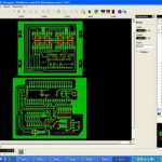
To ensure that a PCB design adheres to the specified design rules, designers use PCB Design Rule Checking (DRC) tools. DRC tools automatically analyze the PCB layout and compare it against a set of predefined rules, flagging any violations or potential issues.
Most PCB design software packages include built-in DRC tools, which can be customized to match the specific requirements of a given project or manufacturing process. By running DRC checks regularly throughout the design process, designers can identify and correct issues early, reducing the risk of costly redesigns or manufacturing delays.
Frequently Asked Questions (FAQ)
-
Q: What is the difference between trace width and trace spacing?
A: Trace width refers to the thickness of the copper tracks on the PCB, while trace spacing refers to the distance between adjacent traces. Both parameters are critical for ensuring proper signal integrity and manufacturability. -
Q: Why is via size and spacing important in PCB design?
A: Via size and spacing affect the PCB’s manufacturability and signal integrity. Vias that are too small or closely spaced can lead to manufacturing issues, such as drill breakage or incomplete plating. Properly sized and spaced vias ensure reliable connections between layers and minimize signal distortion. -
Q: What is the purpose of power and ground planes in PCB design?
A: Power and ground planes provide a low-impedance path for power distribution and signal return, helping to maintain signal integrity and minimize electromagnetic interference (EMI). By using dedicated planes rather than traces, designers can ensure a more stable and efficient power distribution network. -
Q: What are some key considerations for high-speed PCB design?
A: When designing PCBs for high-speed applications, key considerations include impedance matching, length matching, differential routing, and proper grounding and shielding. These techniques help minimize signal distortion, crosstalk, and EMI, ensuring reliable performance in high-frequency environments. -
Q: How can PCB Design Rule Checking (DRC) tools help in the design process?
A: PCB Design Rule Checking (DRC) tools automatically analyze the PCB layout and compare it against a set of predefined rules, flagging any violations or potential issues. By running DRC checks regularly throughout the design process, designers can identify and correct issues early, reducing the risk of costly redesigns or manufacturing delays.
Conclusion
PCB design rules are essential guidelines that ensure the proper functionality, manufacturability, and reliability of printed circuit boards. By following these rules, designers can create PCBs that are efficient, cost-effective, and meet the specific requirements of their applications.
Key design rules to consider include minimum trace width and spacing, via size and spacing, component placement and orientation, power and ground plane design, and silkscreen and solder mask specifications. Advanced design considerations, such as high-speed signal integrity and thermal management, may require additional rules and techniques.
To ensure compliance with design rules, designers rely on PCB Design Rule Checking (DRC) tools, which automatically analyze the PCB layout and flag any violations or potential issues. By adhering to these rules and best practices, designers can create high-quality PCBs that perform reliably and meet the demands of modern electronic systems.
Leave a Reply