Understanding BGA Solderability
Ball Grid Array (BGA) is a surface-mount packaging used for integrated circuits. BGAs are used to permanently mount devices such as microprocessors. A BGA can provide more interconnection pins than can be put on a dual in-line or flat package. The whole bottom surface of the device can be used, instead of just the perimeter.
What is BGA Solderability?
BGA solderability refers to the ability of the BGA package to form a reliable solder joint with the printed circuit board (PCB) during the assembly process. It is a critical factor in determining the reliability and performance of electronic devices.
Factors Affecting BGA Solderability
Several factors can affect BGA solderability, including:
- Surface finish: The surface finish of the BGA package and PCB pads can significantly impact solderability. Common surface finishes include:
- Immersion Silver (ImAg)
- Electroless Nickel Immersion Gold (ENIG)
-
Organic Solderability Preservative (OSP)
-
Storage conditions: Improper storage of BGA packages, such as exposure to high humidity or temperature, can lead to oxidation and degradation of the surface finish, reducing solderability.
-
Reflow profile: The reflow soldering profile, including peak temperature, time above liquidus, and cooling rate, must be optimized to ensure proper solder joint formation.
-
Solder paste: The quality and consistency of the solder paste used in the assembly process can affect solderability. Factors such as particle size, flux activity, and viscosity must be considered.
BGA Solderability Testing Methods
To ensure the solderability of BGA packages, various testing methods have been developed. These methods help evaluate the wettability and joint formation of BGAs under different conditions.
Wetting Balance Test (WBT)
The Wetting Balance Test is a quantitative method for assessing the solderability of BGA packages. In this test, a BGA ball is dipped into a molten solder bath, and the wetting force is measured as a function of time. Key parameters include:
- Wetting time: The time required for the solder to wet the surface of the BGA ball.
- Maximum wetting force: The maximum force exerted on the BGA ball during the wetting process.
- Wetting angle: The angle formed between the solder and the BGA ball surface.
| Parameter | Acceptable Range |
|---|---|
| Wetting time | < 2 seconds |
| Maximum wetting force | > 2 mN |
| Wetting angle | < 60 degrees |
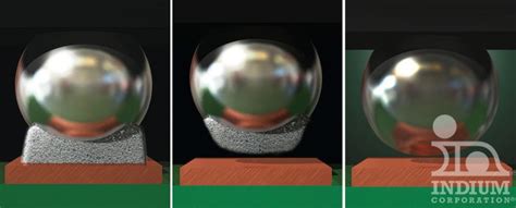
Dip and Look Test
The Dip and Look test is a qualitative method for assessing BGA solderability. In this test, the BGA package is dipped into a molten solder bath for a specified time and then removed. The solder coverage and joint formation are visually inspected using a microscope. Key aspects to consider include:
- Solder coverage: The percentage of the BGA ball surface covered by solder.
- Joint formation: The shape and integrity of the solder joint.
| Aspect | Acceptable Criteria |
|---|---|
| Solder coverage | > 95% of the BGA ball surface covered |
| Joint formation | Smooth, uniform, and free of voids or cracks |
X-ray Inspection
X-ray inspection is a non-destructive method for evaluating the internal structure of BGA solder joints. It allows for the detection of voids, cracks, and other defects that may not be visible through external inspection. Key aspects to consider include:
- Void percentage: The percentage of the solder joint volume occupied by voids.
- Void distribution: The location and size of voids within the solder joint.
| Aspect | Acceptable Criteria |
|---|---|
| Void percentage | < 25% of the solder joint volume |
| Void distribution | No large, concentrated voids near critical areas |

BGA Solderability Standards
Several industry standards have been developed to ensure consistent and reliable BGA solderability. These standards provide guidelines for testing methods, acceptance criteria, and sample preparation.
IPC J-STD-002
IPC J-STD-002, “Solderability Tests for Component Leads, Terminations, Lugs, Terminals and Wires,” is a widely used standard for assessing the solderability of electronic components, including BGAs. It covers various testing methods, such as the Wetting Balance Test and Dip and Look Test, and provides acceptance criteria for each method.
IPC J-STD-003
IPC J-STD-003, “Solderability Tests for Printed Boards,” is a standard specifically focused on the solderability of printed circuit boards. It includes guidelines for sample preparation, testing methods, and acceptance criteria for PCB solderability.
IEC 60068-2-58
IEC 60068-2-58, “Environmental testing – Part 2-58: Tests – Test Td: Test methods for solderability, resistance to dissolution of metallization and to soldering heat of surface mounting devices (SMD),” is an international standard that provides testing methods and acceptance criteria for the solderability of surface-mount devices, including BGAs.

Ensuring BGA Solderability in Manufacturing
To ensure the solderability of BGA packages in the manufacturing process, several best practices should be followed:
-
Proper storage and handling: BGA packages should be stored in a controlled environment with low humidity and temperature to prevent oxidation and degradation of the surface finish. Proper handling techniques, such as using ESD-safe gloves and bags, should be employed to minimize damage.
-
Process control: The assembly process, including solder paste printing, component placement, and reflow soldering, must be carefully controlled and monitored. Regular maintenance and calibration of equipment are essential to ensure consistent results.
-
Incoming inspection: Incoming BGA packages should be inspected for solderability using appropriate testing methods, such as the Wetting Balance Test or Dip and Look Test. This helps identify any potential issues before the components are used in the assembly process.
-
Reflow profile optimization: The reflow soldering profile must be optimized for the specific BGA package and PCB design. Factors such as peak temperature, time above liquidus, and cooling rate should be carefully controlled to ensure proper solder joint formation.
-
Post-assembly inspection: After the assembly process, BGA solder joints should be inspected using methods such as X-ray inspection to detect any defects or anomalies. This allows for timely corrective actions to be taken before the devices are shipped to customers.

Frequently Asked Questions (FAQ)
-
Q: What is the difference between BGA and other surface-mount packages?
A: BGA packages differ from other surface-mount packages, such as QFPs or SOICs, in that they use an array of solder balls underneath the package instead of leads around the perimeter. This allows for a higher pin count and improved electrical and thermal performance. -
Q: Can BGA packages be reworked if solderability issues are encountered?
A: Yes, BGA packages can be reworked using specialized equipment and techniques. However, rework should be avoided whenever possible, as it can be time-consuming and may introduce additional defects. It is always better to ensure proper solderability through process control and incoming inspection. -
Q: How does the surface finish affect BGA solderability?
A: The surface finish of the BGA package and PCB pads can significantly impact solderability. Different surface finishes have varying wetting characteristics and shelf life. For example, ENIG provides excellent solderability but may be prone to “black pad” issues, while OSP has a limited shelf life but is more cost-effective. -
Q: What are the most common defects encountered in BGA soldering?
A: Common defects in BGA soldering include voids, head-in-pillow (HIP), non-wet opens, and bridging. Voids are gaps or cavities within the solder joint, while HIP occurs when the solder ball does not collapse completely during reflow. Non-wet opens are caused by poor wetting of the solder to the pad, and bridging is the formation of unintended connections between adjacent solder balls. -
Q: How can BGA solderability be improved in the design stage?
A: BGA solderability can be improved in the design stage by considering factors such as pad size, spacing, and surface finish. Proper pad design ensures adequate solder joint formation and minimizes the risk of defects. Additionally, choosing a compatible surface finish for both the BGA package and PCB pads can enhance solderability.
In conclusion, BGA solderability is a critical factor in ensuring the reliability and performance of electronic devices. By understanding the factors affecting solderability, employing appropriate testing methods, and following industry standards and best practices, manufacturers can consistently produce high-quality BGA solder joints. Regular process control, incoming inspection, and post-assembly inspection are essential to identify and address any solderability issues promptly. As technology advances and package sizes continue to shrink, maintaining excellent BGA solderability will remain a key challenge and focus for the electronics industry.


Leave a Reply