Introduction to PCB-Phone Technology
In the rapidly evolving world of mobile technology, the printed circuit board (PCB) plays a crucial role in the functionality and performance of smartphones. The PCB-Phone, a class carrier mobile phone PCB, represents a significant advancement in the field, offering enhanced features and capabilities that cater to the growing demands of modern users.
What is a PCB-Phone?
A PCB-Phone is a specialized type of printed circuit board designed specifically for use in mobile phones. It serves as the backbone of the device, connecting and integrating various components such as the processor, memory, storage, and communication modules. The PCB-Phone is characterized by its compact size, high-density layout, and advanced manufacturing techniques that enable it to deliver optimal performance within the limited space available in a smartphone.
The Role of PCB-Phone in Mobile Technology
The PCB-Phone plays a vital role in the overall functioning of a mobile device. It acts as the central hub that facilitates communication between different components and ensures smooth operation of the phone. Some of the key functions of a PCB-Phone include:
-
Signal Routing: The PCB-Phone is responsible for routing electrical signals between various components, allowing for seamless data transfer and communication within the device.
-
Power Distribution: It efficiently distributes power from the battery to all the components, ensuring stable and reliable operation.
-
Component Integration: The PCB-Phone provides a platform for integrating multiple components, such as the processor, memory chips, and sensors, into a cohesive system.
-
Thermal Management: With the increasing power demands of modern smartphones, effective thermal management is crucial. The PCB-Phone incorporates heat dissipation techniques to prevent overheating and ensure optimal performance.
Advancements in PCB-Phone Technology
High-Density Interconnect (HDI) PCBs
One of the major advancements in PCB-Phone technology is the adoption of High-Density Interconnect (HDI) PCBs. HDI PCBs feature smaller trace widths, reduced via sizes, and higher layer counts compared to traditional PCBs. This allows for greater component density and more efficient use of space, enabling manufacturers to pack more features and functionality into smaller form factors.
HDI PCBs offer several advantages for mobile phone applications:
- Miniaturization: HDI technology enables the creation of smaller and thinner PCBs, contributing to the overall reduction in phone size and weight.
- Enhanced Signal Integrity: The smaller traces and reduced via sizes in HDI PCBs minimize signal loss and improve signal integrity, resulting in better performance and reliability.
- Increased Functionality: With the ability to accommodate more components and circuitry, HDI PCBs enable the integration of advanced features such as 5G connectivity, high-resolution cameras, and AI capabilities.
Multi-Layer Stackup
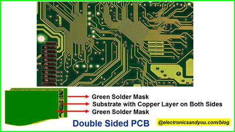
Another significant advancement in PCB-Phone technology is the use of multi-layer stackups. Traditional PCBs typically consist of two or four layers, but modern PCB-Phones often employ eight or more layers to accommodate the increasing complexity of smartphone designs.
Multi-layer stackups offer several benefits:
- Increased Routing Density: With multiple layers available for signal routing, designers can achieve higher routing density and more efficient use of space.
- Improved Signal Integrity: The additional layers provide better shielding and isolation between signals, reducing crosstalk and electromagnetic interference (EMI).
- Enhanced Power Distribution: Dedicated power and ground planes in multi-layer stackups ensure stable and uniform power distribution to all components.
Advanced Materials and Manufacturing Processes
PCB-Phone technology has also benefited from advancements in materials and manufacturing processes. The use of high-performance substrate materials, such as low-loss dielectrics and high-conductivity copper, has improved the electrical characteristics and reliability of PCB-Phones.
Additionally, advanced manufacturing techniques, such as precise laser drilling and high-resolution patterning, have enabled the fabrication of ultra-fine features and high-density interconnects. These advancements have contributed to the miniaturization and performance improvements seen in modern smartphones.
Key Components of a PCB-Phone
A typical PCB-Phone consists of several key components that work together to enable the functionality of a smartphone. Let’s take a closer look at some of these components:
Application Processor (AP)
The application processor, also known as the system-on-chip (SoC), is the heart of a smartphone. It integrates the central processing unit (CPU), graphics processing unit (GPU), and various other subsystems into a single chip. The AP is responsible for executing the phone’s operating system, running applications, and handling tasks such as image and video processing.
Memory (RAM and Storage)
Memory is an essential component of a PCB-Phone, as it stores and provides quick access to data and instructions required by the AP. There are two main types of memory in a smartphone:
-
Random Access Memory (RAM): RAM is volatile memory that temporarily stores data and instructions currently in use by the AP. It enables fast access and multitasking capabilities.
-
Storage: Non-volatile storage, typically in the form of flash memory or an embedded multimedia card (eMMC), holds the phone’s operating system, applications, and user data even when the device is powered off.
Connectivity Modules
Connectivity modules enable a smartphone to communicate with the outside world. Some of the key connectivity components on a PCB-Phone include:
-
Cellular Modem: The cellular modem handles voice calls and data transmission over cellular networks such as 4G LTE or 5G.
-
Wi-Fi and Bluetooth: Integrated Wi-Fi and Bluetooth modules allow the phone to connect to wireless networks and exchange data with other devices.
-
GPS: The Global Positioning System (GPS) module enables location-based services and navigation capabilities.
Power Management IC (PMIC)
The power management integrated circuit (PMIC) is responsible for managing and distributing power to various components on the PCB-Phone. It regulates voltage levels, controls battery charging, and implements power-saving techniques to optimize battery life.
Sensors and Peripherals
Modern smartphones incorporate a wide range of sensors and peripherals to enhance user experience and enable advanced features. Some common sensors found on a PCB-Phone include:
- Accelerometer and Gyroscope: These sensors detect the phone’s orientation and motion, enabling features like screen rotation and gesture recognition.
- Proximity and Ambient Light Sensors: These sensors detect the phone’s proximity to objects and adjust the display brightness based on ambient lighting conditions.
- Fingerprint Sensor: Integrated fingerprint sensors provide secure authentication and unlock capabilities.

PCB-Phone Design Considerations
Designing a PCB-Phone involves several key considerations to ensure optimal performance, reliability, and manufacturability. Let’s explore some of these considerations:
Signal Integrity
Maintaining signal integrity is crucial in PCB-Phone design to ensure reliable communication between components and minimize signal degradation. Some strategies for improving signal integrity include:
- Impedance Matching: Matching the impedance of signal traces to the characteristic impedance of the components and connectors minimizes reflections and signal distortions.
- Shielding: Implementing proper shielding techniques, such as ground planes and via stitching, helps reduce electromagnetic interference (EMI) and crosstalk between signals.
- Length Matching: Ensuring equal lengths for critical signal paths, such as differential pairs, minimizes skew and maintains signal synchronization.
Power Integrity
Proper power distribution is essential for the stable and reliable operation of a PCB-Phone. Key considerations for power integrity include:
- Power Plane Design: Implementing dedicated power planes and utilizing proper power plane shapes and sizes helps minimize voltage drops and ensure uniform power distribution.
- Decoupling Capacitors: Placing decoupling capacitors close to power-hungry components, such as the AP and memory, helps suppress voltage fluctuations and maintain a stable power supply.
- Power Sequencing: Ensuring the correct power-up and power-down sequences for different components helps prevent voltage spikes and protects sensitive circuitry.
Thermal Management
With the increasing power demands of modern smartphones, effective thermal management is crucial to prevent overheating and ensure optimal performance. Some thermal management techniques used in PCB-Phone design include:
- Thermal Vias: Placing thermal vias near heat-generating components helps dissipate heat from the PCB to the phone’s chassis or heatsink.
- Copper Pours: Using large copper pours on the PCB layers helps spread heat evenly and improves thermal conductivity.
- Component Placement: Strategic placement of components, considering their heat generation and dissipation characteristics, helps optimize thermal distribution and prevent hot spots.
Manufacturing Considerations
Designing a PCB-Phone also involves considering manufacturing constraints and ensuring the design is optimized for mass production. Some key manufacturing considerations include:
- Design for Manufacturing (DFM): Adhering to DFM guidelines, such as minimum trace widths, clearances, and via sizes, helps ensure the PCB-Phone can be reliably manufactured at scale.
- Panelization: Optimizing the PCB-Phone layout for panelization, which involves arranging multiple PCBs on a larger panel for efficient fabrication, helps reduce manufacturing costs and improve yield.
- Testing and Inspection: Incorporating testability features, such as test points and boundary scan, facilitates automated testing and inspection processes, ensuring the quality and reliability of the manufactured PCB-Phones.
Future Trends in PCB-Phone Technology
As mobile technology continues to evolve, PCB-Phone technology must adapt to keep pace with the ever-increasing demands for performance, functionality, and efficiency. Some of the future trends in PCB-Phone technology include:
5G and Beyond
The adoption of 5G networks is driving the development of advanced PCB-Phone designs that can support the higher frequencies and bandwidths required for 5G connectivity. This includes the integration of 5G modems, antennae, and RF front-end modules into the PCB-Phone layout.
Looking beyond 5G, researchers are already exploring the potential of 6G networks, which are expected to offer even higher data rates, lower latencies, and enhanced connectivity. PCB-Phone technology will need to evolve to accommodate the requirements of these future networks.
Flexible and Foldable Designs
The emergence of flexible and foldable smartphones has introduced new challenges and opportunities for PCB-Phone design. Flexible PCBs, which can bend and conform to the shape of the device, are becoming increasingly important in enabling these innovative form factors.
Designing PCB-Phones for flexible and foldable devices requires careful consideration of material selection, component placement, and mechanical stress management. Advancements in materials science, such as the development of flexible substrates and stretchable conductors, will play a crucial role in realizing the potential of these designs.
Integration of Advanced Sensors
As smartphones become more intelligent and feature-rich, the integration of advanced sensors into PCB-Phones will continue to be a key focus. This includes the incorporation of high-resolution cameras, 3D sensing modules, and biometric sensors for enhanced user authentication and experience.
PCB-Phone designs will need to accommodate the specific requirements of these sensors, such as precise alignment, shielding, and signal processing. The integration of AI accelerators and dedicated image signal processors (ISPs) will also become more prevalent to enable on-device processing of sensor data.
Enhanced Power Efficiency
Battery life remains a critical factor in smartphone user satisfaction, and PCB-Phone technology plays a significant role in optimizing power efficiency. Future PCB-Phone designs will focus on implementing advanced power management techniques, such as:
- Dynamic Voltage and Frequency Scaling (DVFS): Dynamically adjusting the voltage and frequency of the AP based on workload demands to minimize power consumption.
- Power Gating: Selectively shutting down unused components or subsystems to reduce leakage power and extend battery life.
- Energy Harvesting: Integrating energy harvesting mechanisms, such as solar cells or piezoelectric generators, into the PCB-Phone to supplement battery power and enable self-sustaining operation.
Frequently Asked Questions (FAQ)
-
What is the difference between a PCB-Phone and a regular PCB?
A PCB-Phone is a specialized type of printed circuit board designed specifically for use in mobile phones. It is characterized by its compact size, high-density layout, and advanced manufacturing techniques that enable it to deliver optimal performance within the limited space available in a smartphone. Regular PCBs, on the other hand, are more general-purpose and may not have the same level of miniaturization and integration as PCB-Phones. -
How does a PCB-Phone contribute to the functionality of a smartphone?
A PCB-Phone serves as the central hub that connects and integrates various components of a smartphone, such as the processor, memory, storage, and communication modules. It is responsible for routing electrical signals, distributing power, and facilitating communication between different components. The PCB-Phone plays a crucial role in enabling the advanced features and capabilities of modern smartphones. -
What are some of the key advancements in PCB-Phone technology?
Some of the key advancements in PCB-Phone technology include the adoption of High-Density Interconnect (HDI) PCBs, which offer greater component density and more efficient use of space; the use of multi-layer stackups for improved signal integrity and power distribution; and the incorporation of advanced materials and manufacturing processes for improved electrical characteristics and reliability. -
What are the main components found on a typical PCB-Phone?
A typical PCB-Phone consists of several key components, including the application processor (AP), which serves as the heart of the smartphone; memory (RAM and storage) for storing data and instructions; connectivity modules such as cellular modems, Wi-Fi, and Bluetooth; power management ICs (PMICs) for managing power distribution; and various sensors and peripherals for enhancing user experience and enabling advanced features. -
What are some of the future trends in PCB-Phone technology?
Some of the future trends in PCB-Phone technology include the adoption of 5G and beyond for higher data rates and enhanced connectivity; the development of flexible and foldable designs to enable innovative form factors; the integration of advanced sensors such as high-resolution cameras and biometric sensors; and a focus on enhanced power efficiency through advanced power management techniques and energy harvesting mechanisms.
| Component | Function |
|---|---|
| Application Processor | Executes the phone’s operating system, runs applications, and handles image/video processing |
| Memory (RAM and Storage) | Stores data and instructions for quick access by the AP |
| Cellular Modem | Handles voice calls and data transmission over cellular networks |
| Wi-Fi and Bluetooth | Enables connection to wireless networks and data exchange with other devices |
| GPS | Provides location-based services and navigation capabilities |
| Power Management IC | Manages and distributes power to various components on the PCB-Phone |
| Sensors and Peripherals | Enhance user experience and enable advanced features (e.g., accelerometer, fingerprint sensor) |
Conclusion
The PCB-Phone, as a class carrier mobile phone PCB, represents a significant advancement in mobile technology. Its compact size, high-density layout, and advanced manufacturing techniques enable it to deliver optimal performance and functionality within the limited space of a smartphone.
Through advancements such as HDI PCBs, multi-layer stackups, and the integration of key components like the application processor, memory, and connectivity modules, PCB-Phones have played a crucial role in the evolution of smartphones. They have enabled the miniaturization of devices while simultaneously enhancing features and capabilities.
As mobile technology continues to evolve, PCB-Phone technology must adapt to keep pace with the increasing demands for performance, functionality, and efficiency. Future trends such as 5G and beyond, flexible and foldable designs, integration of advanced sensors, and enhanced power efficiency will shape the development of PCB-Phones in the coming years.
By understanding the intricacies of PCB-Phone technology, designers and manufacturers can create innovative and powerful smartphones that meet the ever-changing needs of consumers. As we move forward, the PCB-Phone will undoubtedly remain at the forefront of mobile technology, driving advancements and enabling the next generation of smartphones.
Leave a Reply