Understanding BGA Packages
What is a BGA?
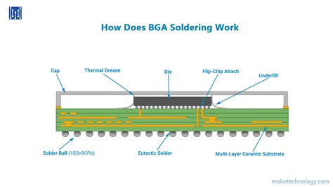
A Ball Grid Array (BGA) is a surface-mount package that utilizes an array of solder balls on the bottom side of the package to establish electrical connections with the PCB. The solder balls are arranged in a grid pattern, allowing for a high density of interconnects in a small footprint.
BGA Package Types
BGAs come in various types and configurations to suit different applications and requirements. Some common BGA package types include:
| Package Type | Description |
|---|---|
| Plastic BGA (PBGA) | Encapsulated in a plastic compound, suitable for low to medium pin counts |
| Ceramic BGA (CBGA) | Uses a ceramic substrate, offers better thermal and electrical performance |
| Fine-pitch BGA (FBGA) | Features a smaller pitch between solder balls, enabling higher pin density |
| Micro BGA (µBGA) | Miniaturized version of BGA, ideal for compact devices and wearables |
BGA Assembly Process
PCB Design Considerations
Designing a PCB for BGA assembly requires careful consideration of several factors:
- Pad Size and Pitch: The pad size and pitch must match the BGA package specifications to ensure proper solder ball alignment and connection.
- Solder Mask Openings: Solder mask openings should be precisely defined to prevent solder bridging and ensure adequate solder joint formation.
- Via-in-Pad: Via-in-pad design, where vias are placed directly under the BGA pads, can be employed to improve routing density and signal integrity.
- Thermal Management: Adequate thermal vias and copper planes should be incorporated to dissipate heat effectively from the BGA package.
Solder Paste Printing
Solder paste printing is a critical step in BGA assembly, as it deposits the solder material onto the PCB pads. The process involves using a stencil with apertures that match the BGA pad layout. The solder paste is then applied onto the stencil and transferred to the PCB using a squeegee.
| Parameter | Typical Value |
|---|---|
| Stencil Thickness | 0.1 mm to 0.15 mm |
| Aperture Size | 80% to 90% of pad size |
| Solder Paste Type | Type 3 or Type 4 (particle size) |
BGA Placement
Once the solder paste is applied, the BGA package is placed onto the PCB using a pick-and-place machine. The machine uses vision systems and precise placement heads to align the BGA package with the pads on the PCB. Accurate placement is crucial to ensure proper solder joint formation and avoid misalignment-related defects.
Reflow Soldering
Reflow soldering is the process of melting the solder paste to form permanent solder joints between the BGA package and the PCB. The assembLED PCB is passed through a reflow oven, which follows a specific temperature profile to melt the solder, allow it to wet the surfaces, and then cool down to form solid joints.
| Reflow Profile Parameter | Typical Value |
|---|---|
| Preheat Temperature | 150°C to 180°C |
| Soak Time | 60 to 120 seconds |
| Peak Temperature | 235°C to 245°C |
| Time Above Liquidus (TAL) | 60 to 90 seconds |
Inspection and Testing
After the reflow process, the assembled PCBs undergo inspection and testing to verify the quality and reliability of the BGA solder joints. Various inspection methods can be employed:
- X-ray Inspection: X-ray imaging allows non-destructive inspection of the solder joints, detecting voids, bridging, or missing balls.
- Automated Optical Inspection (AOI): AOI systems use high-resolution cameras and image processing algorithms to detect surface-level defects.
- Electrical Testing: Functional testing and boundary-scan testing can be performed to verify the electrical integrity of the BGA connections.

BGA Assembly Equipment
To achieve high-quality BGA assembly, specialized equipment is required at various stages of the process:
Solder Paste Printer
A solder paste printer is used to apply the solder paste onto the PCB pads through a stencil. Key features of a solder paste printer include:
- Adjustable squeegee pressure and speed
- Vision system for stencil alignment
- Substrate support and clamping mechanism
- Print area size and resolution
Pick-and-Place Machine
A pick-and-place machine is responsible for accurately placing the BGA package onto the PCB. Important considerations for a pick-and-place machine include:
- Placement accuracy and repeatability
- Vision system for component alignment
- Nozzle types and sizes for handling different BGA packages
- Placement speed and throughput
Reflow Oven
A reflow oven is used to melt the solder paste and form the solder joints between the BGA package and the PCB. Key features of a reflow oven include:
- Temperature profiling capabilities
- Heating zones and control
- Cooling rate and convection
- Nitrogen atmosphere compatibility
Inspection Systems
Inspection systems are used to verify the quality of the BGA solder joints after the reflow process. Various inspection systems include:
- X-ray inspection systems
- Automated optical inspection (AOI) systems
- 3D solder paste inspection (SPI) systems

BGA Assembly Challenges and Best Practices
Warpage Control
BGA packages and PCBs are prone to warpage due to thermal stresses during the reflow process. Warpage can lead to open or inadequate solder joints. To mitigate warpage:
- Use low-CTE (Coefficient of Thermal Expansion) PCB materials
- Implement proper PCB design techniques, such as symmetric layer stackup and balanced copper distribution
- Control reflow temperature profile to minimize thermal gradients
Solder Joint Reliability
Ensuring the reliability of BGA solder joints is critical for the long-term performance of the assembled PCBs. Best practices for improving solder joint reliability include:
- Selecting compatible solder paste and surface finish materials
- Optimizing reflow temperature profile for proper solder wetting and intermetallic compound (IMC) formation
- Incorporating underfill material to redistribute stresses and enhance mechanical strength
Rework and Repair
In case of defects or failures, BGA Rework and repair may be necessary. Rework and repair processes involve:
- Localized heating to remove the defective BGA package without damaging the PCB
- Cleaning and preparing the site for replacement
- Precise alignment and placement of the new BGA package
- Controlled reflow to form new solder joints
Specialized rework stations and skilled operators are required to perform BGA rework successfully.

Frequently Asked Questions (FAQ)
1. What is the difference between BGA and QFN packages?
BGA (Ball Grid Array) and QFN (Quad Flat No-lead) are both surface-mount package types, but they have distinct differences:
- BGA packages have an array of solder balls on the bottom side for electrical connections, while QFN packages have flat contact pads along the perimeter.
- BGA packages offer higher pin density and better thermal dissipation compared to QFN packages.
- QFN packages have a smaller footprint and lower profile than BGA packages, making them suitable for space-constrained applications.
2. Can BGA packages be assembled using lead-free solder?
Yes, BGA packages can be assembled using lead-free solder. In fact, the electronics industry has largely transitioned to lead-free solder materials to comply with RoHS (Restriction of Hazardous Substances) regulations. Common lead-free solder alloys used for BGA assembly include SAC305 (Sn96.5Ag3.0Cu0.5) and SAC405 (Sn95.5Ag4.0Cu0.5).
3. What is the typical pitch size for BGA packages?
The pitch size of BGA packages varies depending on the package type and pin count. Common pitch sizes for BGA packages include:
- 1.27 mm (50 mil)
- 1.00 mm (39 mil)
- 0.80 mm (31 mil)
- 0.65 mm (26 mil)
- 0.50 mm (20 mil)
Smaller pitch sizes, such as 0.40 mm and 0.35 mm, are also used in high-density BGA packages.
4. How can voids in BGA solder joints be minimized?
Voids in BGA solder joints can be minimized through various techniques:
- Optimizing the solder paste printing process to ensure consistent and adequate solder volume
- Using a nitrogen atmosphere during reflow to reduce oxidation and improve solder wetting
- Implementing a proper reflow temperature profile with adequate soak time and peak temperature
- Selecting compatible solder paste and surface finish materials to promote good solder flow and wetting
Additionally, using vacuum reflow soldering can significantly reduce void formation in BGA solder joints.
5. What is the purpose of underfill in BGA assembly?
Underfill is an epoxy-based material that is applied between the BGA package and the PCB after the reflow process. The purpose of underfill is to:
- Redistribute stresses and reduce the strain on the solder joints caused by thermal expansion mismatches
- Enhance the mechanical strength and reliability of the BGA solder joints
- Provide additional protection against moisture, contaminants, and mechanical shock
Underfill is especially critical for large BGA packages and applications exposed to harsh environmental conditions.
Conclusion
BGA assembly capabilities have greatly expanded the possibilities in electronIC Packaging and assembly. By understanding the intricacies of the BGA assembly process, including PCB design considerations, solder paste printing, BGA placement, reflow soldering, and inspection techniques, manufacturers can achieve reliable and high-quality BGA assemblies. Investing in the right equipment, such as solder paste printers, pick-and-place machines, reflow ovens, and inspection systems, is crucial to ensure consistent and efficient BGA assembly.
However, BGA assembly also presents challenges, such as warpage control and solder joint reliability. By implementing best practices, such as selecting compatible materials, optimizing reflow profiles, and incorporating underfill, these challenges can be effectively addressed.
As technology advances and device miniaturization continues, BGA assembly capabilities will remain a critical aspect of electronics manufacturing. Staying updated with the latest techniques, materials, and equipment is essential for companies to stay competitive and meet the evolving demands of the industry.


Leave a Reply