Introduction to PCB Stack-up
A printed circuit board (PCB) stack-up refers to the arrangement of copper layers and insulating materials that make up a PCB. The stack-up determines the electrical properties, signal integrity, and manufacturability of the board. As PCBs become more complex, with higher layer counts and increased density, understanding and designing an appropriate stack-up becomes crucial for ensuring optimal performance and reliability.
In this article, we will focus on 10-layer PCB stack-ups, providing comprehensive guides on how to design and optimize them for various applications. We will cover the following topics:
- The importance of PCB stack-up design
- Types of materials used in PCB stack-ups
- Signal integrity considerations
- Power delivery and ground planes
- Impedance control and matching
- Manufacturability and cost considerations
- Examples of 10-layer PCB stack-ups for different applications
- Frequently asked questions (FAQ) about 10-layer PCB stack-ups
The Importance of PCB Stack-up Design
A well-designed PCB stack-up is essential for several reasons:
-
Signal integrity: The arrangement of layers and the choice of materials affect the signal quality, including crosstalk, reflections, and electromagnetic interference (EMI).
-
Power delivery: The placement and thickness of power and ground planes impact the ability to deliver clean, stable power to components.
-
Impedance control: Achieving the desired impedance for transmission lines is crucial for high-speed signals and depends on the stack-up design.
-
Manufacturability: The stack-up must be feasible to manufacture, considering factors such as layer registration, drilling, and lamination.
-
Cost: The choice of materials and the number of layers directly influence the cost of the PCB.
Types of Materials Used in PCB Stack-ups
The materials used in a PCB stack-up play a critical role in determining its electrical and mechanical properties. The most common materials include:
Copper
Copper is used for the conductive layers in a PCB. The thickness of the copper is typically measured in ounces per square foot (oz/ft²), with common thicknesses being 0.5 oz/ft², 1 oz/ft², and 2 oz/ft².
FR-4
FR-4 is the most widely used insulating material in PCBs. It is a composite material made of woven fiberglass cloth with an epoxy resin binder. FR-4 has good mechanical strength, thermal stability, and electrical insulation properties.
High-frequency laminates
For applications requiring better signal integrity and lower losses at high frequencies, specialized laminates such as Rogers, Isola, or Nelco materials may be used. These materials have lower dielectric constants and dissipation factors compared to FR-4.
Prepreg
Prepreg (pre-impregnated) is a partially cured composite material used to bond the layers of a PCB together during the lamination process. The choice of prepreg material and thickness affects the overall thickness and dielectric properties of the stack-up.

Signal Integrity Considerations
Signal integrity is a critical aspect of PCB design, especially for high-speed digital circuits. The stack-up plays a significant role in maintaining signal integrity by:
-
Minimizing crosstalk: Proper spacing between signal layers and the use of ground planes can help reduce crosstalk between adjacent traces.
-
Controlling impedance: The stack-up design determines the characteristic impedance of transmission lines, which must be controlled to prevent reflections and ensure proper signal termination.
-
Reducing EMI: Appropriate layer arrangement and the use of ground planes can help minimize electromagnetic interference (EMI) and reduce the risk of signal degradation.
Power Delivery and Ground Planes
Power delivery and ground planes are essential for providing a stable and clean power supply to components on the PCB. In a 10-layer stack-up, it is common to dedicate multiple layers to power and ground planes.
The placement and thickness of these planes are crucial for several reasons:
-
Lowering impedance: Thicker planes and shorter distances between power and ground planes help reduce the impedance of the power delivery network, ensuring a stable supply voltage.
-
Reducing voltage drop: Adequate copper thickness and proper placement of power planes minimize voltage drop across the board, ensuring that components receive the required voltage levels.
-
Providing shielding: Ground planes act as shields between signal layers, reducing crosstalk and EMI.
-
Facilitating return paths: Ground planes provide low-impedance return paths for high-speed signals, reducing loop area and minimizing inductance.
Impedance Control and Matching
Controlling and matching the impedance of transmission lines is essential for maintaining signal integrity in high-speed designs. The stack-up design directly affects the characteristic impedance of the transmission lines, which depends on factors such as:
- Dielectric constant of the insulating material
- Thickness of the insulating layer
- Width of the trace
- Copper thickness
To achieve the desired impedance, designers must carefully choose the appropriate materials and geometries for the stack-up. Common impedance values for high-speed designs include 50Ω, 75Ω, and 100Ω.
Impedance matching is also crucial for preventing reflections and ensuring proper signal termination. This can be achieved through techniques such as:
- Trace width control: Adjusting the width of the traces to match the desired impedance.
- Differential pair routing: Using coupled traces with a specific spacing to achieve differential impedance.
- Termination resistors: Placing resistors at the end of transmission lines to match the characteristic impedance and prevent reflections.
Manufacturability and Cost Considerations
When designing a 10-layer PCB stack-up, it is essential to consider manufacturability and cost factors:
-
Layer registration: Ensuring that the layers align properly during the lamination process is crucial for maintaining signal integrity and preventing manufacturing defects.
-
Drilling and via formation: The stack-up design must account for the feasibility of drilling through-holes and vias, considering aspects such as aspect ratios and minimum hole sizes.
-
Material availability: Choosing materials that are readily available and compatible with the manufacturing process can help reduce lead times and costs.
-
Yields: A well-designed stack-up can improve manufacturing yields by minimizing the risk of defects and ensuring the board’s reliability.
-
Cost: The choice of materials, the number of layers, and the required manufacturing processes all impact the overall cost of the PCB. Striking a balance between performance and cost is essential for successful PCB design.
Examples of 10-Layer PCB Stack-ups for Different Applications
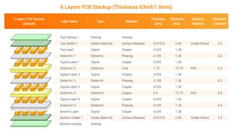
To illustrate the concepts discussed in this article, let’s look at some examples of 10-layer PCB stack-ups for different applications.
Example 1: High-Speed Digital Design
In this example, we will consider a 10-layer PCB stack-up for a high-speed digital design with a mix of signal layers, power planes, and ground planes.
| Layer | Material | Thickness (mm) | Function |
|---|---|---|---|
| 1 | FR-4 | 0.10 | Signal |
| 2 | FR-4 | 0.20 | Ground |
| 3 | FR-4 | 0.10 | Signal |
| 4 | FR-4 | 0.20 | Power |
| 5 | FR-4 | 0.10 | Signal |
| 6 | FR-4 | 0.20 | Ground |
| 7 | FR-4 | 0.10 | Signal |
| 8 | FR-4 | 0.20 | Power |
| 9 | FR-4 | 0.10 | Signal |
| 10 | FR-4 | 0.10 | Signal |
This stack-up provides a good balance between signal integrity and power delivery. The ground planes on layers 2 and 6 provide shielding between the signal layers, reducing crosstalk and EMI. The power planes on layers 4 and 8 ensure a stable power supply to the components.
Example 2: RF Design
For an RF design, the stack-up may use high-frequency laminates to reduce losses and maintain signal integrity at higher frequencies.
| Layer | Material | Thickness (mm) | Function |
|---|---|---|---|
| 1 | Rogers | 0.10 | Signal |
| 2 | Rogers | 0.20 | Ground |
| 3 | Rogers | 0.10 | Signal |
| 4 | FR-4 | 0.20 | Power |
| 5 | FR-4 | 0.10 | Signal |
| 6 | FR-4 | 0.20 | Ground |
| 7 | FR-4 | 0.10 | Signal |
| 8 | FR-4 | 0.20 | Power |
| 9 | Rogers | 0.10 | Signal |
| 10 | Rogers | 0.10 | Signal |
In this stack-up, the outer layers and the layers adjacent to the ground planes use Rogers material, which has better high-frequency performance compared to FR-4. This helps maintain signal integrity for the RF signals.
Frequently Asked Questions (FAQ)
-
Q: What is the minimum recommended thickness for a power or ground plane in a 10-layer PCB stack-up?
A: The minimum recommended thickness for a power or ground plane is typically 0.5 oz/ft² (0.017 mm). However, thicker planes may be necessary for high-current applications or to reduce voltage drop across the board. -
Q: Can I use different materials for different layers in a 10-layer PCB stack-up?
A: Yes, it is possible to use different materials for different layers in a 10-layer PCB stack-up. This is often done to optimize the performance of certain layers, such as using high-frequency laminates for RF signal layers or using thicker FR-4 for power and ground planes. -
Q: How do I determine the appropriate trace width and spacing for a given impedance in a 10-layer PCB stack-up?
A: To determine the appropriate trace width and spacing for a given impedance, you can use impedance calculators or simulation tools that take into account the dielectric constant of the insulating material, the thickness of the dielectric layer, and the copper thickness. Many PCB design software packages include built-in tools for calculating impedance based on the stack-up and trace geometry. -
Q: What are the advantages of using a 10-layer PCB stack-up compared to fewer layers?
A: Using a 10-layer PCB stack-up offers several advantages, including: - More space for routing signals, power, and ground
- Better signal integrity due to the ability to use more ground planes and shielding
- Improved power delivery with dedicated power planes
-
Increased flexibility for complex designs with high component density
-
Q: How does the choice of prepreg material affect the performance of a 10-layer PCB stack-up?
A: The choice of prepreg material can affect the performance of a 10-layer PCB stack-up in several ways: - Dielectric constant: The dielectric constant of the prepreg material influences the characteristic impedance of the transmission lines and the signal propagation speed.
- Thickness: The thickness of the prepreg layers affects the overall thickness of the PCB and the spacing between layers, which can impact signal integrity and impedance control.
- Thermal stability: The thermal stability of the prepreg material is important for maintaining the mechanical and electrical properties of the PCB over its operating temperature range.
Conclusion
Designing a 10-layer PCB stack-up requires careful consideration of signal integrity, power delivery, impedance control, manufacturability, and cost factors. By understanding the principles and best practices outlined in this article, designers can create stack-ups that are optimized for their specific applications and requirements.
Remember that the stack-up design is just one aspect of the overall PCB design process, and it must be integrated with other design considerations, such as component placement, routing, and thermal management. Collaboration between the PCB designer, the electrical engineer, and the manufacturing team is essential for ensuring the success of the final product.
As PCB technology continues to evolve, with higher speeds, greater densities, and more complex architectures, the importance of a well-designed stack-up will only continue to grow. By staying up-to-date with the latest materials, techniques, and tools, designers can create 10-layer PCB stack-ups that push the boundaries of performance and reliability.

Leave a Reply