What are Gerber Files?
Gerber files are a standard file format used in the printed circuit board (PCB) industry to describe the layout of a PCB. They contain information about the copper layers, solder mask, silk screen, and drill holes of a PCB design. Gerber files are essential for manufacturing PCBs as they provide the necessary data for the fabrication process.
What is Panelization?
Panelization is the process of arranging multiple PCB designs on a single panel for manufacturing. This is done to optimize the use of the PCB material and reduce production costs. By panelizing Gerber files, you can combine several smaller PCB designs into a larger panel, making the manufacturing process more efficient.
Benefits of Panelization
- Cost reduction: Panelizing PCBs allows for more efficient use of materials and reduces the overall cost per PCB.
- Faster production: Manufacturing panels with multiple PCBs is faster than producing individual boards separately.
- Consistent quality: Panelizing ensures that all the PCBs on a panel are manufactured under the same conditions, resulting in consistent quality.

How to Panelize gerber Files
Step 1: Prepare Your Gerber Files
Before panelizing, ensure that your Gerber files are complete and error-free. Check that all the necessary layers are included and that the files adhere to the Gerber format specifications. It’s also a good idea to review your PCB design for any potential issues that may arise during manufacturing.
Step 2: Choose a Panelization Software
There are several software options available for panelizing Gerber files. Some popular choices include:
- GerberPanelizer
- PCB Panelizer
- CAM350
- PentaLogix ViewMate
Choose a software that suits your needs and budget. Some software may offer additional features like automatic panelization or design rule checks.
Step 3: Import Your Gerber Files
Import your Gerber files into the panelization software. Most software will allow you to import multiple Gerber files at once, making it easy to panelize several PCB designs simultaneously.
Step 4: Arrange the PCBs on the Panel
Arrange the PCBs on the panel in a way that optimizes material usage and minimizes waste. Consider the following factors when arranging the PCBs:
- Panel size: Choose a panel size that accommodates all your PCBs efficiently.
- Spacing: Ensure adequate spacing between the PCBs to allow for cutting and handling during manufacturing.
- Orientation: Orient the PCBs in a way that minimizes the number of cuts required to separate them from the panel.
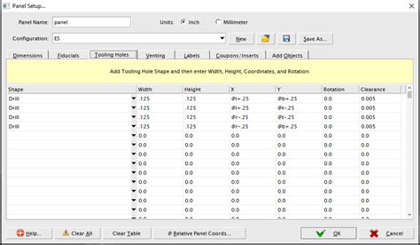
Step 5: Add Tooling and Fiducial Marks
Tooling and fiducial marks are essential for the manufacturing process. They help align the panel during fabrication and assembly. Add these marks to your panel according to your manufacturer’s specifications.
- Tooling holes: These are used to secure the panel during manufacturing and should be placed in the corners of the panel.
- Fiducial marks: These are used for alignment during the assembly process and should be placed near each PCB on the panel.
Step 6: Add Mousebites or V-Scoring
Mousebites or V-scoring are methods used to separate the individual PCBs from the panel after manufacturing. Choose the appropriate method based on your PCB design and manufacturer’s recommendations.
- Mousebites: These are small, perforated tabs that connect the PCBs to the panel. They can be easily broken off after manufacturing.
- V-scoring: This method involves cutting a V-shaped groove along the edges of each PCB, making it easy to snap them apart from the panel.
Step 7: Generate the Panelized Gerber Files
Once you have arranged your PCBs and added all the necessary marks and features, generate the panelized Gerber files. Most panelization software will allow you to export the files in the same format as your original Gerber files.
Step 8: Verify and Send to Manufacturer
Before sending your panelized Gerber files to your manufacturer, verify that all the information is correct and that the files meet their specifications. Double-check the following:
- File format: Ensure that the panelized Gerber files are in the correct format required by your manufacturer.
- Layer information: Verify that all the necessary layers are included and properly labeled.
- Dimensions: Check that the panel size and PCB dimensions are accurate.
Once you have verified the panelized Gerber files, send them to your manufacturer for fabrication.

Best Practices for Panelizing Gerber Files
- Keep your PCB designs simple and standardized to make panelization easier.
- Use a consistent naming convention for your Gerber files to avoid confusion.
- Communicate with your manufacturer to ensure that your panelized Gerber files meet their requirements.
- Test your panelized design before mass production to identify any potential issues.
- Optimize your panel layout to minimize material waste and reduce costs.

Frequently Asked Questions (FAQ)
1. Can I panelize Gerber files manually?
While it is possible to panelize Gerber files manually, it is not recommended. Manual panelization is time-consuming and prone to errors. Using dedicated panelization software is more efficient and ensures accurate results.
2. How much space should I leave between PCBs on a panel?
The spacing between PCBs on a panel depends on various factors, such as the PCB size, manufacturing process, and the separator method used. As a general rule, aim for a spacing of at least 2-3 mm between PCBs. Always consult your manufacturer for their specific requirements.
3. What is the difference between mousebites and V-scoring?
Mousebites are small, perforated tabs that connect the PCBs to the panel, while V-scoring involves cutting a V-shaped groove along the edges of each PCB. Mousebites are more common for smaller PCBs, while V-scoring is often used for larger or thicker boards. The choice between the two depends on your PCB design and manufacturer’s preferences.
4. Can I panelize different PCB designs on the same panel?
Yes, you can panelize different PCB designs on the same panel, as long as they share the same material and thickness specifications. This is known as mixed panelization and can help optimize material usage and reduce costs. However, ensure that your manufacturer can accommodate mixed panels in their production process.
5. What should I do if my manufacturer rejects my panelized Gerber files?
If your manufacturer rejects your panelized Gerber files, the first step is to communicate with them to understand the reason for the rejection. Common issues include incorrect file formats, missing layers, or non-compliance with their design specifications. Once you have identified the problem, make the necessary corrections and resubmit the files. Maintaining clear communication with your manufacturer can help avoid such issues in the future.
| Aspect | Description |
|---|---|
| Gerber Files | Standard file format used in the PCB industry to describe the layout of a PCB |
| Panelization | The process of arranging multiple PCB designs on a single panel for manufacturing |
| Benefits | Cost reduction, faster production, consistent quality |
| Panelization Software | GerberPanelizer, PCB Panelizer, CAM350, PentaLogix ViewMate |
| Tooling Marks | Used to secure the panel during manufacturing, placed in the corners of the panel |
| Fiducial Marks | Used for alignment during the assembly process, placed near each PCB on the panel |
| Mousebites | Small, perforated tabs that connect the PCBs to the panel, easily broken off after manufacturing |
| V-scoring | Cutting a V-shaped groove along the edges of each PCB, making it easy to snap them apart from the panel |
By following these steps and best practices, you can successfully panelize your Gerber files and optimize your PCB manufacturing process. Remember to maintain clear communication with your manufacturer and test your panelized design before mass production to ensure the best possible results.


Leave a Reply