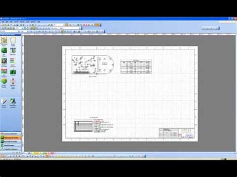
Introduction to PCB Fabrication Drawings
A PCB fabrication drawing, also known as a PCB fab drawing or PCB manufacturing drawing, is a crucial document that provides all the necessary information for the manufacturer to produce a printed circuit board (PCB) according to the designer’s specifications. It contains detailed instructions on the board’s dimensions, materials, layer stackup, component placement, and other essential aspects of the PCB fabrication process.
Understanding how to read and interpret a PCB fabrication drawing is essential for both PCB designers and manufacturers. It ensures that the design intent is clearly communicated and that the final product meets the required specifications. In this article, we will dive deep into the various elements of a PCB fabrication drawing and provide a comprehensive guide on how to read and understand them.
Key Elements of a PCB Fabrication Drawing
A typical PCB fabrication drawing consists of several key elements that provide a complete overview of the board’s design and manufacturing requirements. These elements include:
- Title Block
- Board Outline and Dimensions
- Layer Stackup
- Drill Drawing
- Silkscreen and Legend
- Fabrication Notes
- Revision History
Let’s explore each of these elements in detail.
Title Block
The title block is usually located in the bottom right corner of the fabrication drawing and contains essential information about the PCB, such as:
- Part Number or Drawing Number
- Revision Number
- Date of Creation or Last Modification
- Company Name or Logo
- Designer’s Name or Initials
- Page Number (if the drawing spans multiple pages)
This information helps in identifying the specific version of the PCB and tracking any changes made to the design.
Board Outline and Dimensions
The board outline is a graphical representation of the PCB’s physical shape and size. It includes the overall dimensions of the board, as well as any cutouts, notches, or special features. The dimensions are typically provided in both metric (mm) and imperial (inches) units to accommodate different manufacturing preferences.
In addition to the outer dimensions, the drawing may also specify the board thickness, corner radii, and any required tolerances. These details ensure that the manufactured board fits perfectly into its intended enclosure or system.
Layer Stackup
The layer stackup section of the fabrication drawing provides a cross-sectional view of the PCB, showing the arrangement and thickness of each copper layer, insulating substrate, and any special materials used. It also specifies the material type and thickness for each layer, such as FR-4, Rogers, or high-frequency laminates.
The layer stackup is crucial for determining the board’s electrical properties, impedance control, and manufacturability. It helps the manufacturer choose the appropriate materials and processes to ensure the PCB meets the design requirements.
| Layer | Material | Thickness (mm) | Copper Weight (oz) |
|---|---|---|---|
| Top Copper | FR-4 | 0.035 | 1 |
| Dielectric 1 | FR-4 | 0.2 | – |
| Inner Copper 1 | FR-4 | 0.035 | 1 |
| Dielectric 2 | FR-4 | 0.2 | – |
| Inner Copper 2 | FR-4 | 0.035 | 1 |
| Dielectric 3 | FR-4 | 0.2 | – |
| Bottom Copper | FR-4 | 0.035 | 1 |
Example of a 4-layer PCB stackup table
Drill Drawing
The drill drawing section specifies the location, size, and type of all the holes required on the PCB. This includes:
- Plated Through Holes (PTHs) for component leads and vias
- Non-Plated Through Holes (NPTHs) for mounting or mechanical purposes
- Blind and Buried Vias (if applicable)
The drill sizes are usually provided in a table format, with each size assigned a unique symbol or code. The drawing may also include the drill tolerances and any special requirements for hole plating or via filling.
| Symbol | Drill Size (mm) | Tolerance (mm) | Plating |
|---|---|---|---|
| A | 0.8 | ±0.05 | Plated |
| B | 1.0 | ±0.05 | Plated |
| C | 1.2 | ±0.05 | Plated |
| D | 2.5 | ±0.1 | Non-Plated |
Example of a drill size table
Silkscreen and Legend
The silkscreen and legend section of the fabrication drawing provides information on the text, logos, and other markings to be printed on the PCB surface. This includes:
- Component outlines and reference designators
- Polarity markers and pin 1 indicators
- Test points and fiducial markers
- Warning labels and regulatory markings
- Company logos and branding elements
The drawing specifies the color, size, and location of each silkscreen element, as well as any special requirements for the font or artwork.
Fabrication Notes
Fabrication notes are additional instructions or specifications that are not covered in the other sections of the drawing. These may include:
- Surface finish requirements (e.g., HASL, ENIG, OSP)
- Soldermask color and type
- Impedance control requirements
- Special handling or packaging instructions
- Any other custom or non-standard specifications
The fabrication notes ensure that the manufacturer has all the necessary information to produce the PCB according to the designer’s intent.
Revision History
The revision history section tracks any changes made to the PCB design over time. It typically includes:
- Revision number or letter
- Date of the revision
- Brief description of the changes made
- Initials of the person who made the changes
Maintaining an accurate revision history is essential for version control and ensuring that all stakeholders are working with the most up-to-date design.

How to Interpret a PCB Fabrication Drawing
Now that we have covered the key elements of a PCB fabrication drawing, let’s discuss how to interpret the information provided and use it to ensure a successful manufacturing process.
-
Start by reviewing the title block to identify the specific PCB design and version you are working with. Make sure all the information is accurate and up to date.
-
Next, examine the board outline and dimensions to ensure that the PCB will fit into its intended enclosure or system. Pay attention to any special features or tolerances specified in the drawing.
-
Study the layer stackup to understand the arrangement and properties of each layer in the PCB. Verify that the materials and thicknesses specified meet your design requirements and are compatible with your manufacturing processes.
-
Review the drill drawing to ensure that all the necessary holes are accounted for and sized correctly. Check that the plating and tolerances specified are appropriate for your manufacturing capabilities.
-
Examine the silkscreen and legend section to verify that all the required markings and labels are included and positioned correctly. Ensure that the artwork meets your quality and branding standards.
-
Carefully read through the fabrication notes to identify any special requirements or instructions that may impact the manufacturing process. Make sure you can accommodate these requirements or discuss any concerns with the PCB designer.
-
Finally, check the revision history to ensure that you are working with the most current version of the design. If there are any discrepancies or questions, consult with the PCB designer or the appropriate stakeholders to resolve them before proceeding with manufacturing.
By thoroughly reviewing and interpreting each section of the PCB fabrication drawing, you can ensure that the manufactured board meets all the design requirements and functions as intended.

Common Challenges and Best Practices
While PCB fabrication drawings provide a wealth of information, there are some common challenges and best practices to keep in mind when working with them:
-
Inconsistencies or errors in the drawing can lead to manufacturing issues or delays. It is essential to thoroughly review the drawing and communicate any concerns or questions to the PCB designer before starting production.
-
Outdated or incomplete information can also cause problems. Ensure that you are working with the most recent version of the fabrication drawing and that all the necessary details are provided.
-
Custom or non-standard requirements may require additional communication and coordination between the PCB designer and manufacturer. Make sure to discuss any special needs or constraints early in the process to avoid potential issues.
-
Maintaining clear and consistent communication throughout the manufacturing process is crucial. If any changes or updates are made to the design, ensure that all stakeholders are informed and that the fabrication drawing is revised accordingly.
-
Using standardized formats and templates for PCB fabrication drawings can help ensure consistency and clarity. Consider developing a set of internal guidelines or adopting industry standards, such as the IPC-D-325 standard for PCB documentation.
By following these best practices and maintaining a thorough understanding of PCB fabrication drawings, you can streamline the manufacturing process and ensure the production of high-quality, reliable PCBs.

Frequently Asked Questions (FAQ)
-
What is the purpose of a PCB fabrication drawing?
A PCB fabrication drawing provides a detailed visual representation of a printed circuit board design, including all the necessary information for manufacturing, such as dimensions, layer stackup, drill holes, and silkscreen markings. -
What are the key elements of a PCB fabrication drawing?
The key elements of a PCB fabrication drawing include the title block, board outline and dimensions, layer stackup, drill drawing, silkscreen and legend, fabrication notes, and revision history. -
Why is the layer stackup important in a PCB fabrication drawing?
The layer stackup provides a cross-sectional view of the PCB, showing the arrangement and thickness of each copper layer, insulating substrate, and any special materials used. It is crucial for determining the board’s electrical properties, impedance control, and manufacturability. -
How can I ensure that I am working with the most up-to-date version of a PCB fabrication drawing?
To ensure that you are working with the most current version of a PCB fabrication drawing, check the revision history section, which tracks any changes made to the design over time. If there are any discrepancies or questions, consult with the PCB designer or the appropriate stakeholders. -
What should I do if I encounter custom or non-standard requirements in a PCB fabrication drawing?
If you encounter custom or non-standard requirements in a PCB fabrication drawing, discuss them with the PCB designer as early as possible in the manufacturing process. Clear and consistent communication is essential to ensure that all requirements are understood and accommodated.
Conclusion
PCB fabrication drawings are essential tools for communicating design intent and ensuring the successful manufacture of printed circuit boards. By understanding the key elements of a fabrication drawing and how to interpret them, PCB designers and manufacturers can work together to produce high-quality, reliable PCBs that meet all the necessary requirements.
Throughout this article, we have provided a comprehensive guide on how to read and understand PCB fabrication drawings. We have covered the various elements, such as the title block, board outline and dimensions, layer stackup, drill drawing, silkscreen and legend, fabrication notes, and revision history. We have also discussed common challenges and best practices to keep in mind when working with these drawings.
By following the guidelines and best practices outlined in this article, you can streamline your PCB manufacturing process, reduce errors and delays, and ensure that your PCBs meet the highest standards of quality and reliability. Remember to maintain clear and consistent communication with all stakeholders, and always work with the most up-to-date version of the fabrication drawing.
As PCB designs continue to evolve and become more complex, the importance of accurate and comprehensive fabrication drawings will only continue to grow. By mastering the art of reading and interpreting these drawings, you can position yourself as a valuable asset in the world of PCB design and manufacturing.


Leave a Reply