Introduction to PCB etching
Printed Circuit Board (PCB) etching is a crucial process in the manufacturing of electronic devices. It involves the removal of unwanted copper from a PCB substrate to create the desired circuit pattern. The process of PCB etching requires skill, precision, and the right tools to achieve the best results. In this article, we will explore the process of PCB etching and how to test your etching chops by creating a PCB map.
What is PCB Etching?
PCB etching is the process of removing unwanted copper from a PCB substrate to create the desired circuit pattern. The process involves applying a resist layer to the copper surface of the PCB, exposing it to light through a photomask, and then developing the resist to reveal the desired circuit pattern. The exposed copper is then removed using an etching solution, leaving behind the desired circuit pattern.
Why is PCB Etching Important?
PCB etching is an essential step in the manufacturing of electronic devices. It allows for the creation of complex circuit patterns on a small scale, enabling the development of compact and efficient electronic devices. Without PCB etching, it would be impossible to create the intricate circuit patterns required for modern electronic devices.
Tools and Materials Required for PCB Etching
To successfully etch a PCB, you will need the following tools and materials:
| Tool/Material | Description |
|---|---|
| PCB substrate | The base material on which the circuit pattern will be etched |
| Photoresist | A light-sensitive material used to create the circuit pattern |
| Photomask | A transparent sheet with the desired circuit pattern printed on it |
| Exposure unit | A device used to expose the photoresist to light through the photomask |
| Developer | A solution used to develop the exposed photoresist |
| Etching solution | A solution used to remove the unwanted copper from the PCB substrate |
| Etching tank | A container used to hold the etching solution and PCB substrate during the etching process |
| Protective gear | Gloves, goggles, and an apron to protect yourself from the etching solution |
Choosing the Right PCB Substrate
The choice of PCB substrate is crucial to the success of the etching process. The most common PCB substrates are:
- FR4: A glass-reinforced epoxy laminate that is widely used in the electronics industry due to its excellent mechanical and electrical properties.
- Polyimide: A high-performance polymer that is used in applications that require high temperature resistance and flexibility.
- Aluminum: A metal substrate that is used in applications that require high thermal conductivity and heat dissipation.
When choosing a PCB substrate, consider the following factors:
- The intended application of the PCB
- The required electrical and mechanical properties
- The cost and availability of the substrate
Selecting the Right Photoresist
Photoresist is a light-sensitive material used to create the desired circuit pattern on the PCB substrate. There are two types of photoresist:
- Positive photoresist: Exposed areas become soluble in the developer solution and are removed during development.
- Negative photoresist: Exposed areas become insoluble in the developer solution and remain on the PCB substrate after development.
When selecting a photoresist, consider the following factors:
- The type of PCB substrate being used
- The resolution and aspect ratio required for the circuit pattern
- The ease of use and availability of the photoresist
Choosing the Right Etching Solution
The etching solution is used to remove the unwanted copper from the PCB substrate. There are several types of etching solutions available, including:
- Ferric chloride: A popular etching solution that is relatively safe and easy to use.
- Ammonium persulfate: A fast-acting etching solution that produces high-quality results but can be more difficult to control.
- Cupric chloride: An etching solution that is often used in industrial settings due to its high etch rate and ability to produce fine features.
When choosing an etching solution, consider the following factors:
- The type of PCB substrate being used
- The required etch rate and resolution
- The safety and environmental considerations of the solution

The PCB Etching Process
The PCB etching process involves several steps, each of which must be performed carefully to achieve the best results.
Step 1: Preparing the PCB Substrate
Before etching, the PCB substrate must be cleaned and prepared for the photoresist application. This involves:
- Cleaning the substrate with a degreaser to remove any dirt, oil, or contaminants
- Roughening the surface of the substrate with sandpaper or a chemical treatment to improve adhesion of the photoresist
- Applying a thin layer of photoresist to the substrate using a spin coater or spray coater
Step 2: Exposing the Photoresist
Once the photoresist has been applied, it must be exposed to light through the photomask to create the desired circuit pattern. This involves:
- Aligning the photomask with the PCB substrate
- Placing the substrate and photomask in an exposure unit
- Exposing the photoresist to light for a specific amount of time, depending on the type of photoresist and exposure unit being used
Step 3: Developing the Photoresist
After exposure, the photoresist must be developed to reveal the desired circuit pattern. This involves:
- Immersing the PCB substrate in a developer solution for a specific amount of time
- Rinsing the substrate with water to remove any excess developer
- Inspecting the substrate to ensure that the desired circuit pattern has been successfully developed
Step 4: Etching the PCB
Once the photoresist has been developed, the PCB substrate is ready for etching. This involves:
- Placing the substrate in an etching tank filled with the chosen etching solution
- Agitating the solution to ensure even etching across the substrate
- Monitoring the etching process to ensure that the desired amount of copper is removed
- Removing the substrate from the etching tank and rinsing it with water to stop the etching process
Step 5: Removing the Photoresist
After etching, the remaining photoresist must be removed from the PCB substrate. This involves:
- Immersing the substrate in a photoresist stripper solution
- Rinsing the substrate with water to remove any excess stripper
- Inspecting the substrate to ensure that all of the photoresist has been successfully removed

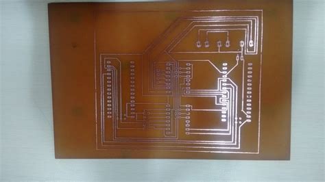
Testing Your Etching Chops with PCB Map Making
One way to test your etching chops is by creating a PCB map. A PCB map is a visual representation of the circuit pattern on a PCB substrate. Creating a PCB map requires careful planning and execution, and can be a good way to practice your etching skills.
Step 1: Designing the Circuit Pattern
The first step in creating a PCB map is to design the circuit pattern. This can be done using PCB design software or by hand-drawing the pattern on paper. When designing the pattern, consider the following factors:
- The size and shape of the PCB substrate
- The number and location of components on the PCB
- The required trace widths and spacing
- Any special features or requirements of the circuit
Step 2: Creating the Photomask
Once the circuit pattern has been designed, the next step is to create the photomask. This can be done using a laser printer or by hand-drawing the pattern on a transparent sheet. When creating the photomask, consider the following factors:
- The type of photoresist being used (positive or negative)
- The required resolution and accuracy of the pattern
- The orientation and alignment of the pattern on the PCB substrate
Step 3: Etching the PCB Map
With the photomask created, the next step is to etch the PCB map. This involves following the same steps as described in the PCB etching process above, but with a few additional considerations:
- The PCB map should be etched on a high-quality PCB substrate to ensure the best results
- The etching time and solution concentration may need to be adjusted to achieve the desired level of detail and resolution
- The PCB map should be carefully inspected after etching to ensure that the desired pattern has been successfully transferred to the substrate
Step 4: Evaluating the Results
After etching the PCB map, the final step is to evaluate the results. This involves:
- Inspecting the PCB map for any defects or errors in the etched pattern
- Measuring the trace widths and spacing to ensure that they meet the required specifications
- Testing the electrical continuity and functionality of the PCB map, if applicable
By carefully evaluating the results of the PCB map, you can identify areas where your etching skills need improvement and make adjustments to your process accordingly.

FAQ
- What is the difference between positive and negative photoresist?
-
Positive photoresist becomes soluble in developer solution when exposed to light, while negative photoresist becomes insoluble when exposed to light. Positive photoresist is more commonly used in PCB etching due to its higher resolution and ease of use.
-
Can I use any type of paper for the photomask?
-
No, regular paper is not suitable for use as a photomask due to its opacity and tendency to absorb moisture. Transparency film or specially-coated paper should be used instead to ensure optimal results.
-
How do I know when the etching process is complete?
-
The etching process is complete when all of the unwanted copper has been removed from the PCB substrate, revealing the desired circuit pattern. This can be determined by visually inspecting the substrate and measuring the trace widths and spacing.
-
What should I do if the etched pattern is not as expected?
-
If the etched pattern is not as expected, there are several possible causes, including incorrect exposure time, incorrect developer concentration, or incorrect etching time or solution concentration. To troubleshoot, carefully review each step of the process and make adjustments as needed.
-
Can I reuse the etching solution?
- Yes, etching solution can be reused multiple times, but its effectiveness will diminish over time as the copper concentration increases. It is important to regularly test the solution and replace it as needed to ensure optimal results.
Conclusion
PCB etching is a critical process in the manufacturing of electronic devices, requiring skill, precision, and the right tools and materials. By understanding the basics of PCB etching and practicing your skills through PCB map making, you can improve your etching chops and create high-quality PCBs for a wide range of applications.


Leave a Reply