Introduction to PCB Soldering
Printed Circuit Board (PCB) soldering is a crucial process in the manufacturing of electronic devices. It involves joining electronic components to the PCB using a molten metal alloy called solder. The soldering process ensures electrical connectivity and mechanical stability of the components on the board. In this article, we will discuss the various methods and process flows involved in PCB chip package soldering.
Types of PCB Soldering
There are three main types of PCB soldering:
- Through-hole soldering
- Surface mount soldering
- Mixed technology soldering
Through-hole Soldering
Through-hole soldering is the traditional method of soldering where the components have long leads that are inserted into holes drilled on the PCB. The leads are then soldered to the copper pads on the other side of the board. This method is suitable for larger components and provides a strong mechanical bond.
Surface Mount Soldering
Surface mount soldering, also known as SMT soldering, is a modern technique where the components are placed directly on the surface of the PCB. The components have small metal pads or leads that are soldered to the corresponding pads on the board. SMT soldering allows for smaller components and higher density packaging.
Mixed Technology Soldering
Mixed technology soldering combines both through-hole and surface mount soldering techniques on the same PCB. This method is used when a board requires both types of components for optimal functionality and performance.
PCB Chip Package Soldering Methods
There are several methods used for soldering chip packages onto PCBs. The choice of method depends on factors such as the type of package, the size of the board, and the production volume. Let’s take a look at some of the most common methods.
Wave Soldering
Wave soldering is a fast and efficient method for soldering through-hole components. The process involves passing the PCB over a molten solder wave, which fills the holes and creates a solder joint. The steps involved in wave soldering are as follows:
- Flux application: A thin layer of flux is applied to the bottom side of the PCB to prevent oxidation and improve solder wetting.
- Preheating: The board is preheated to activate the flux and prevent thermal shock during soldering.
- Wave soldering: The board is passed over the solder wave, which fills the holes and creates a solder joint.
- Cooling: The board is cooled to allow the solder to solidify.
Wave soldering is suitable for high-volume production and can handle large components. However, it is not suitable for surface mount components and can cause bridging or short circuits if not properly controlled.
Reflow Soldering
Reflow soldering is the most common method for soldering surface mount components. The process involves applying solder paste to the PCB pads, placing the components, and then heating the board to melt the solder and create a joint. The steps involved in reflow soldering are as follows:
- Solder paste application: Solder paste is applied to the PCB pads using a stencil or screen printing method.
- Component placement: The surface mount components are placed onto the solder paste using a pick-and-place machine or by hand.
- Reflow: The board is heated in a reflow oven, which melts the solder paste and creates a solder joint.
- Cooling: The board is cooled to allow the solder to solidify.
Reflow soldering is suitable for high-volume production and can handle small components with fine pitch leads. However, it requires precise control of the temperature profile and can be affected by factors such as the type of solder paste and the size of the components.
Selective Soldering
Selective soldering is a method used for soldering specific components or areas on a PCB. It involves using a localized heat source, such as a soldering iron or a laser, to melt the solder and create a joint. Selective soldering is suitable for rework or repair operations, or for soldering components that cannot withstand the high temperatures of wave or reflow soldering.
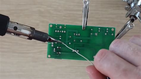
Hand Soldering
Hand soldering is a manual method used for soldering small batches or prototypes. It involves using a soldering iron to apply heat and solder to the component leads and PCB pads. Hand soldering requires skill and experience to achieve consistent and reliable results.

PCB Chip Package Soldering Process Flow
The PCB chip package soldering process flow involves several steps that must be followed in a specific order to ensure a high-quality and reliable solder joint. The steps are as follows:
- PCB Design and Fabrication
- The PCB is designed using CAD software and fabricated according to the specifications.
-
The board is cleaned and inspected for defects.
-
Solder Paste Application
- Solder paste is applied to the PCB pads using a stencil or screen printing method.
-
The thickness and consistency of the solder paste are critical for achieving a good solder joint.
-
Component Placement
- The components are placed onto the solder paste using a pick-and-place machine or by hand.
-
The placement accuracy and orientation of the components are crucial for proper soldering.
-
Reflow Soldering
- The board is heated in a reflow oven according to a specific temperature profile.
- The solder paste melts and creates a solder joint between the component leads and the PCB pads.
-
The board is cooled to allow the solder to solidify.
-
Inspection and Testing
- The soldered board is inspected visually and using X-ray or automated optical inspection (AOI) equipment.
-
The board is tested for functionality and performance.
-
Rework and Repair
- If any defects or issues are found during inspection or testing, the board may need to be reworked or repaired.
- Selective soldering or hand soldering may be used for rework or repair operations.

Factors Affecting PCB Chip Package Soldering Quality
Several factors can affect the quality and reliability of PCB chip package soldering. These include:
- Solder paste quality: The type, composition, and viscosity of the solder paste can affect the soldering process and the final joint quality.
- Reflow temperature profile: The temperature profile used during reflow soldering must be carefully controlled to ensure proper melting and wetting of the solder.
- Component placement accuracy: The placement accuracy and orientation of the components can affect the soldering process and the final joint quality.
- PCB design and layout: The design and layout of the PCB, including the pad size, shape, and spacing, can affect the soldering process and the final joint quality.
- Cleanliness: The cleanliness of the PCB and components is critical for achieving a good solder joint. Contamination or oxidation can prevent proper wetting and bonding of the solder.

Common PCB Chip Package Soldering Defects
Despite careful control of the soldering process, defects can still occur. Some common defects include:
- Bridging: Solder bridging occurs when solder inadvertently connects two or more adjacent pads or leads.
- Insufficient solder: Insufficient solder can result in a weak or open joint that may fail under stress or vibration.
- Excess solder: Excess solder can cause shorts or bridging between adjacent pads or leads.
- Cold joint: A cold joint occurs when the solder does not melt completely or when there is insufficient wetting of the surfaces. Cold joints are weak and prone to failure.
- Tombstoning: Tombstoning occurs when a component stands up on one end due to uneven heating or surface tension during reflow soldering.
Best Practices for PCB Chip Package Soldering
To ensure high-quality and reliable PCB chip package soldering, follow these best practices:
- Use high-quality solder paste and components.
- Ensure proper storage and handling of solder paste to prevent contamination or degradation.
- Use a stencil or screen with the appropriate thickness and aperture size for solder paste application.
- Ensure accurate placement and orientation of components using a pick-and-place machine or by hand.
- Use a reflow oven with a carefully controlled temperature profile.
- Keep the PCB and components clean and free from contamination or oxidation.
- Inspect the soldered board visually and using X-ray or AOI equipment.
- Test the board for functionality and performance.
- Use selective soldering or hand soldering for rework or repair operations.
FAQs
- What is the difference between wave soldering and reflow soldering?
-
Wave soldering is used for through-hole components, while reflow soldering is used for surface mount components. Wave soldering involves passing the board over a molten solder wave, while reflow soldering involves applying solder paste and heating the board to melt the solder.
-
What is solder paste, and why is it used in PCB soldering?
-
Solder paste is a mixture of tiny solder particles suspended in a flux medium. It is used in reflow soldering to apply solder to the PCB pads and component leads. The flux helps to clean and activate the surfaces for better solder wetting and bonding.
-
What is the purpose of the reflow temperature profile in PCB soldering?
-
The reflow temperature profile is a carefully controlled sequence of heating and cooling stages used during reflow soldering. It ensures that the solder paste melts and wets the surfaces properly, and that the solder joint solidifies without defects or damage to the components.
-
How can PCB soldering defects be prevented or minimized?
-
PCB soldering defects can be prevented or minimized by using high-quality materials, ensuring proper storage and handling of solder paste, using appropriate stencils or screens for solder paste application, ensuring accurate placement and orientation of components, using a carefully controlled reflow temperature profile, keeping the PCB and components clean, and inspecting and testing the soldered board.
-
What is selective soldering, and when is it used in PCB soldering?
- Selective soldering is a method used for soldering specific components or areas on a PCB using a localized heat source, such as a soldering iron or a laser. It is used for rework or repair operations, or for soldering components that cannot withstand the high temperatures of wave or reflow soldering.
Conclusion
PCB chip package soldering is a critical process in the manufacturing of electronic devices. It involves joining electronic components to the PCB using a molten metal alloy called solder. There are several methods and process flows used for PCB soldering, including wave soldering, reflow soldering, selective soldering, and hand soldering. The choice of method depends on factors such as the type of package, the size of the board, and the production volume.
To ensure high-quality and reliable PCB chip package soldering, it is important to follow best practices such as using high-quality materials, ensuring proper storage and handling of solder paste, using appropriate stencils or screens for solder paste application, ensuring accurate placement and orientation of components, using a carefully controlled reflow temperature profile, keeping the PCB and components clean, and inspecting and testing the soldered board.
By understanding the various methods and process flows involved in PCB chip package soldering, and by following best practices and minimizing defects, manufacturers can produce high-quality and reliable electronic devices that meet the demands of today’s market.


Leave a Reply