What are Castellated Pads?
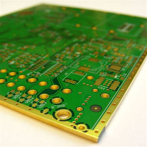
Castellated pads, also known as castellations or castellated holes, are a type of surface mount pad used in printed circuit board (PCB) design. They consist of semi-circular notches or “castles” cut into the edges of a PCB, with each notch having a copper pad for soldering components or connecting to other boards.
Castellated pads provide a simple and compact method for joining PCBs at right angles to form multi-board assemblies. The castellation notches allow solder to wick between boards during reflow soldering, creating strong mechanical and electrical connections.
Advantages of Using Castellated Holes
There are several benefits to using castellated pads in PCB designs:
-
Space savings – Castellations enable high-density perpendicular board-to-board connections without additional connectors or wiring. This minimizes space requirements and allows for more compact assemblies.
-
Cost reduction – Fewer components and connectors are needed with castellated connections, which lowers material and assembly costs compared to other joining methods. The PCB panels themselves form the castellated features.
-
Reliability – Castellated connections create robust solder joints with large surface areas. The solder can wick between notches for added strength. Connections can withstand significant mechanical stress and vibration.
-
Modularity – Uniform castellated modules can be reconfigured and connected in various orientations. This allows for design flexibility and potential reuse of modular subsystems across projects.
-
Signal integrity – Castellations provide short, direct paths between boards. This minimizes signal reflections, crosstalk, and noise that can occur with longer traces, cables or connectors, benefiting high-speed designs.
Castellation Fabrication Process
Castellated pads are formed during the PCB fabrication process using specialized drill and routing techniques:
-
Drilling – Precisely located holes are drilled where the castellation notches will be located, typically using a CNC drill machine. The hole diameter is slightly smaller than the final castellation size.
-
Routing – A V-shaped routing tool cuts a semi-circular groove from the hole to the board edge. This forms the distinctive castle shape. The router bit has a specific angle (often 45°) to create the desired notch geometry.
-
Plating – The drilled holes and routed notches are then plated with copper to form conductive pads for soldering. Additional surface finishes like ENIG may be applied for oxidation resistance and solderability.
-
Cutting – Individual boards are cut out from the fabricated panel, with the castellations now located along the board edges. V-groove cutting or routing is commonly used to separate the boards while retaining the castellation features.
Proper castellation fabrication requires careful design and precise control of drilling, routing, and plating processes to achieve the desired mechanical fit, solderable surfaces, and impedance characteristics.
Castellation Design Considerations
When designing castellated pads, several key parameters should be considered:
| Parameter | Typical Value | Notes |
|---|---|---|
| Drill Hole Diameter | 0.5-1.0 mm | Smaller than final castellation size |
| Castellation Width | 0.8-1.2 mm | Measured across the notch opening |
| Castellation Depth | 0.4-0.8 mm | Depth of the routed notch |
| Pad Width | 0.6-1.0 mm | Copper pad size for soldering |
| Pad Spacing | 1.0-2.0 mm | Gap between castellated pads |
| Board Thickness | 0.8-1.6 mm | Affects castellation depth and fit |
Designers should also consider the arrangement and spacing of castellated pads to ensure proper alignment and fit between mating boards. Clearances around the castellations are necessary for solder wicking and inspection.
Soldering Castellated Connections
Castellated pads are typically soldered using reflow soldering processes. The PCB modules are aligned and held together with the castellations facing each other. Solder paste is applied to the castellated pads, either manually or using stencils.
During reflow, the solder melts and wicks into the castellation notches through capillary action. The surface tension of the molten solder helps align and hold the boards in place. As the solder cools, it forms a strong mechanical and electrical bond between the mating castellations.
Proper soldering of castellated connections requires well-controlled reflow profiles and precise alignment of the boards. Insufficient solder or poor wetting can result in weak or open connections. Excessive solder can cause bridging or short circuits between adjacent pads.
Inspection of castellated solder joints can be challenging due to the hidden nature of the connections. X-ray imaging or specialized optical techniques may be necessary to verify joint quality and detect any defects.
Castellated Pad Soldering Tips
To achieve reliable castellated solder connections, consider these tips:
-
Solder paste volume – Apply sufficient solder paste to fill the castellation notches and form a robust joint. Stencils or paste dispensing can help control the amount of solder applied.
-
Board alignment – Ensure precise alignment of the castellated pads before soldering. Fixtures or alignment pins can help maintain position during reflow.
-
Reflow profile – Use a well-controlled reflow profile with adequate time above the solder melting point to allow for proper wetting and wicking. Avoid excessive heat which can cause solder defects.
-
Cleaning – Clean any flux residue from the castellated connections after soldering. Leftover flux can be difficult to remove later and may impact joint reliability.
-
Inspection – Perform thorough visual and X-ray inspections to verify joint quality and identify any defects like bridging, voids, or poor wetting. Address any issues before final assembly.

Applications of Castellated Pads
Castellated pads are used in a variety of electronics applications where compact, robust board-to-board connections are required. Some common uses include:
-
Module interconnects – Castellations allow easy interconnection of modular PCB subsystems, such as pluggable sensors, RF modules, or power supplies. Modules can be swapped or upgraded as needed.
-
Vertical board stacking – Castellated pads enable high-density vertical stacking of PCBs to save space in three-dimensional assemblies. This is common in compact devices like smartphones, wearables, or IoT nodes.
-
Edge connector replacement – Castellations can serve as an alternative to traditional edge connector sockets. The PCB itself acts as the “plug” which can be soldered directly to a backplane or motherboard.
-
Mezzanine card mounting – Castellated pads provide a low-profile way to mount mezzanine cards or daughter boards perpendicular to a main board. This allows for modular expansion or configuration options.
-
High-speed interconnects – The short, direct paths provided by castellated connections are well-suited for high-speed signals like DDR memory or SerDes links. The castellations help maintain signal integrity between boards.
Frequently Asked Questions (FAQ)
1. What is the difference between castellated pads and edge connectors?
Castellated pads are a type of surface mount pad that allows direct soldering between boards, while edge connectors use separate socket and plug components for removable connections. Castellations are typically smaller and more compact than edge connectors.
2. Can castellated pads be used for high-current connections?
Castellated pads can handle moderate currents, but the current carrying capacity is limited by the size of the pads and the solder joints. For high-current applications, larger pads, multiple castellation rows, or additional power connectors may be necessary.
3. How do castellated holes affect PCB impedance?
The castellation notches can create discontinuities in PCB traces which can affect impedance matching. Careful design of the castellation geometry and surrounding traces is necessary to minimize impedance mismatches, especially for high-speed signals.
4. What is the minimum pitch for castellated pads?
The minimum pitch depends on the PCB fabrication capabilities and the soldering process. Typical minimum pitches range from 0.4 mm to 1.0 mm. Smaller pitches require precise fabrication and soldering control to avoid bridging or open connections.
5. Can castellated pads be used with surface mount components?
Yes, castellated pads are compatible with surface mount components. The components can be mounted on the same side of the board as the castellations or on the opposite side. Proper layout and spacing is necessary to accommodate both the components and the castellated connections.
Leave a Reply