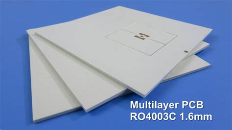
Introduction to Rogers 4003 Material
Rogers 4003 is a popular high-frequency laminate material used in the manufacturing of printed circuit boards (PCBs) for various applications, such as telecommunications, aerospace, and defense. This advanced material offers excellent electrical properties, making it suitable for high-speed digital and RF/microwave applications.
Properties of Rogers 4003
| Property | Value |
|---|---|
| Dielectric Constant (10 GHz) | 3.38 ± 0.05 |
| Dissipation Factor (10 GHz) | 0.0027 |
| Thermal Conductivity | 0.64 W/m/K |
| Coefficient of Thermal Expansion (CTE) | 11-17 ppm/°C |
| Density | 1.79 g/cm³ |
Rogers 4003 exhibits a stable dielectric constant over a wide frequency range, low dissipation factor, and good thermal conductivity. These properties make it an ideal choice for high-frequency PCB designs that require consistent performance and reliability.
PCB Manufacturing Process with Rogers 4003
1. Material Selection and Preparation
The first step in manufacturing a Rogers 4003 PCB is selecting the appropriate copper-clad laminate. The laminate consists of a Rogers 4003 core with copper foil on one or both sides, depending on the design requirements. The copper foil thickness can vary, with common options being 0.5 oz, 1 oz, and 2 oz.
Before processing, the laminate should be properly stored and handled to maintain its quality and prevent damage. Proper storage conditions include a temperature range of 10-30°C and a relative humidity of 50-70%.
2. Drilling
Once the laminate is prepared, the next step is drilling holes for through-hole components and vias. The drilling process for Rogers 4003 is similar to that of other PCB materials, with a few key considerations:
- Use sharp, high-quality carbide drill bits to minimize damage to the material
- Adjust drilling parameters, such as speed and feed rate, to accommodate the material’s properties
- Employ proper cooling and debris removal techniques to prevent overheating and contamination
3. Copper Patterning
After drilling, the copper foil on the laminate is patterned to create the desired circuit layout. There are two primary methods for copper patterning:
a. Subtractive Process (Etching):
– Apply a photoresist layer to the copper surface
– Expose the photoresist using a photomask with the desired circuit pattern
– Develop the photoresist to remove the exposed areas
– Etch away the unwanted copper using a chemical etchant
– Strip the remaining photoresist, leaving the patterned copper traces
b. Additive Process (Plating):
– Apply a thin layer of electroless copper to the laminate surface
– Apply a photoresist layer and expose it using a photomask with the desired circuit pattern
– Develop the photoresist to remove the unexposed areas
– Electroplate additional copper onto the exposed areas to achieve the desired thickness
– Strip the photoresist and etch away the thin electroless copper layer, leaving the patterned copper traces
The choice between subtractive and additive processes depends on factors such as design complexity, feature size, and production volume.
4. Lamination and Multilayer Bonding
For multi-layer Rogers 4003 PCBs, the individual layers need to be laminated together. The lamination process involves the following steps:
- Prepare the inner layers by patterning the copper as described in the previous section
- Apply a layer of prepreg (pre-impregnated) material between the inner layers
- Place the stack of inner layers and prepreg in a lamination press
- Apply heat and pressure according to the manufacturer’s recommendations to bond the layers together
- Allow the laminated board to cool and stabilize
After lamination, additional drilling may be required to create via holes that interconnect the layers.
5. Surface Finish and Solder Mask Application
To protect the copper traces and provide a solderable surface, a solder mask and surface finish are applied to the PCB. The solder mask is a thin, protective layer that covers the copper traces, leaving only the exposed pads for component attachment. The solder mask application process typically involves:
- Applying a liquid photoimageable solder mask to the PCB surface
- Exposing the solder mask using a photomask with the desired openings
- Developing the solder mask to remove the unexposed areas
- Curing the solder mask to achieve the final properties
Common surface finishes for Rogers 4003 PCBs include:
- HASL (Hot Air Solder Leveling)
- ENIG (Electroless Nickel Immersion Gold)
- OSP (Organic Solderability Preservative)
- Immersion Silver
- Immersion Tin
The choice of surface finish depends on factors such as the intended application, solderability requirements, and shelf life.
6. Electrical Testing and Inspection
Before the PCBs are sent for assembly, they undergo thorough electrical testing and inspection to ensure they meet the specified requirements. Some common tests and inspections include:
- Continuity testing to verify the integrity of the copper traces
- Isolation testing to check for shorts between traces
- Impedance testing to confirm the characteristic impedance of controlled-impedance traces
- Visual inspection to check for defects, such as scratches, pinholes, or contamination
- Microsectioning to verify the integrity of vias and plated through-holes
Boards that pass the testing and inspection process are ready for assembly, while those with defects are either reworked or scrapped, depending on the nature and extent of the issues.

PCB Assembly with Rogers 4003
1. Component Selection and Placement
The first step in assembling a Rogers 4003 PCB is selecting the appropriate components based on the design requirements. Components should be chosen considering their compatibility with the high-frequency characteristics of the Rogers 4003 material. Factors such as package type, size, and parasitics should be taken into account.
Once the components are selected, they are placed on the PCB according to the assembly drawing or pick-and-place file. Automated pick-and-place machines are commonly used for high-volume production, while manual placement may be employed for low-volume or prototype builds.
2. Soldering
After component placement, the PCB is ready for soldering. There are two primary soldering methods used for Rogers 4003 PCBs:
a. Reflow Soldering:
– Apply solder paste to the pads using a stencil or screen printing process
– Place the components onto the pads, with the solder paste acting as a temporary adhesive
– Pass the PCB through a reflow oven, which heats the board according to a predetermined temperature profile
– The solder paste melts and forms a metallurgical bond between the component leads and the pads
– Allow the board to cool, solidifying the solder joints
b. Wave Soldering:
– Place the through-hole components into their respective holes on the PCB
– Pass the board over a molten solder wave, which wets the component leads and fills the through-holes
– The solder cools and solidifies, creating a mechanical and electrical connection between the components and the PCB
The choice between reflow and wave soldering depends on the types of components used (surface mount or through-hole) and the design requirements.
3. Cleaning and Inspection
After soldering, the PCBs are cleaned to remove any flux residues or contaminants that may affect the board’s performance or reliability. Cleaning methods include:
- Aqueous cleaning using deionized water and detergents
- Semi-aqueous cleaning using a combination of water and solvents
- Solvent cleaning using chemicals such as isopropyl alcohol or specialty solvents
Once cleaned, the PCBs undergo a final inspection to verify the quality of the solder joints, component placement, and overall assembly. Inspection techniques may include:
- Visual inspection using magnification or automated optical inspection (AOI) systems
- X-ray inspection to check for hidden defects, such as voids or shorts
- Electrical testing to verify the functionality of the assembled board
Boards that pass the inspection process are ready for packaging and shipment, while those with defects are reworked or scrapped, depending on the nature and extent of the issues.

Design Considerations for Rogers 4003 PCBs
When designing PCBs using Rogers 4003 material, there are several key considerations to keep in mind:
1. Controlled Impedance
Rogers 4003 is often used in high-frequency applications where controlled impedance is critical. Designers should carefully calculate the trace widths and spacing to achieve the desired characteristic impedance. Factors such as the dielectric constant, substrate thickness, and copper thickness should be taken into account.
2. Losses and Signal Integrity
At high frequencies, losses and signal integrity issues become more pronounced. Designers should consider the following factors to minimize losses and maintain signal integrity:
- Use wider traces to reduce conductor losses
- Minimize the use of vias, as they can introduce discontinuities and reflections
- Employ proper grounding and shielding techniques to reduce crosstalk and electromagnetic interference (EMI)
- Use appropriate termination techniques, such as matched impedance or series termination, to minimize reflections
3. Thermal Management
Rogers 4003 has a relatively low thermal conductivity compared to other PCB materials, such as aluminum-backed substrates. Designers should consider the power dissipation of the components and the overall thermal profile of the board. Techniques such as using thermal vias, heatsinks, or active cooling may be necessary to ensure proper thermal management.

FAQ
-
Q: What is Rogers 4003, and why is it used in PCB manufacturing?
A: Rogers 4003 is a high-performance laminate material used in the manufacturing of printed circuit boards (PCBs) for high-frequency applications. It offers excellent electrical properties, such as a stable dielectric constant and low dissipation factor, making it suitable for applications in telecommunications, aerospace, and defense. -
Q: What are the key properties of Rogers 4003 that make it suitable for high-frequency PCB designs?
A: Rogers 4003 has a dielectric constant of 3.38 ± 0.05 at 10 GHz and a dissipation factor of 0.0027 at the same frequency. It also exhibits good thermal conductivity (0.64 W/m/K) and a low coefficient of thermal expansion (CTE). These properties contribute to its consistent performance and reliability in high-frequency applications. -
Q: What are the main differences between the subtractive and additive processes for copper patterning in Rogers 4003 PCBs?
A: The subtractive process involves etching away unwanted copper to create the desired circuit pattern, while the additive process involves plating copper onto the laminate surface to build up the circuit pattern. The choice between the two processes depends on factors such as design complexity, feature size, and production volume. -
Q: What are some common surface finishes used for Rogers 4003 PCBs, and how do they differ?
A: Common surface finishes for Rogers 4003 PCBs include HASL (Hot Air Solder Leveling), ENIG (Electroless Nickel Immersion Gold), OSP (Organic Solderability Preservative), Immersion Silver, and Immersion Tin. These finishes differ in terms of their solderable, protection against oxidation, and shelf life. The choice of surface finish depends on the intended application and specific requirements. -
Q: What are some key design considerations when working with Rogers 4003 PCBs?
A: When designing PCBs using Rogers 4003, key considerations include controlled impedance, losses and signal integrity, and thermal management. Designers should carefully calculate trace widths and spacing, minimize the use of vias, employ proper grounding and shielding techniques, and consider the power dissipation of components to ensure optimal performance and reliability.
Conclusion
Rogers 4003 is a high-performance laminate material that offers excellent electrical properties for high-frequency PCB applications. Manufacturing and assembling PCBs using Rogers 4003 requires careful consideration of the material’s properties and the specific design requirements. By following best practices in material selection, processing, and design, engineers can create reliable and high-performing PCBs for demanding applications in telecommunications, aerospace, defense, and other industries.


Leave a Reply