Introduction to SMD Welding
Surface Mount Device (SMD) welding, also known as SMT (Surface Mount Technology) welding, is a crucial process in modern electronics manufacturing. It involves the attachment of small electronic components directly onto the surface of a Printed Circuit Board (PCB). SMD welding has revolutionized the electronics industry by enabling the production of smaller, lighter, and more compact electronic devices. In this comprehensive article, we will delve into the world of SMD welding, exploring its techniques, advantages, challenges, and best practices.
What is SMD Welding?
SMD welding is a process that uses heat to melt and fuse the leads of SMD components to the pads on a PCB. Unlike through-hole technology, where component leads are inserted into holes drilled in the PCB, SMD components are placed directly on the surface of the PCB. This allows for higher component density, improved performance, and reduced manufacturing costs.
Advantages of SMD Welding
- Miniaturization: SMD components are significantly smaller than their through-hole counterparts, enabling the production of more compact and lightweight electronic devices.
- Increased Functionality: With the ability to pack more components onto a single PCB, SMD welding allows for increased functionality and complexity in electronic designs.
- Improved Performance: SMD components have shorter lead lengths, reducing parasitic inductance and capacitance, resulting in improved high-frequency performance and signal integrity.
- Cost-Effective: SMD welding is highly automated, leading to faster assembly times, reduced labor costs, and increased production efficiency.
SMD Welding Techniques
There are several techniques used in SMD welding, each with its own advantages and limitations. Let’s explore the most common SMD welding techniques:
1. Reflow Soldering
Reflow soldering is the most widely used SMD welding technique. It involves applying solder paste, a mixture of tiny solder particles and flux, to the PCB pads using a stencil or screen printing process. SMD components are then placed onto the solder paste using a pick-and-place machine or by hand. The PCB is then subjected to a controlled heating process in a reflow oven, which melts the solder particles and creates a strong bond between the component leads and the PCB pads.
Reflow Soldering Process
- Solder Paste Application: Solder paste is applied to the PCB pads using a stencil or screen printing process.
- Component Placement: SMD components are placed onto the solder paste using a pick-and-place machine or by hand.
- Reflow: The PCB is passed through a reflow oven, which follows a specific temperature profile to melt the solder paste and create a strong bond between the component leads and the PCB pads.
- Cooling: The PCB is allowed to cool, solidifying the solder joints and completing the reflow soldering process.
Advantages of Reflow Soldering
- High-volume production capability
- Consistency and repeatability
- Suitable for a wide range of SMD component sizes and types
- Automated process reduces human error
Challenges of Reflow Soldering
- Requires precise control of the reflow oven temperature profile
- Solder paste shelf life and storage conditions must be carefully managed
- Potential for solder bridges and tombstoning (component lifting) if not properly controlled
2. Wave Soldering
Wave soldering is another common SMD welding technique, particularly suitable for PCBs with a mix of SMD and through-hole components. In wave soldering, the PCB is passed over a molten solder wave, which selectively wets and solders the component leads to the PCB pads.
Wave Soldering Process
- Flux Application: Liquid flux is applied to the bottom side of the PCB to promote solder wetting and prevent oxidation.
- Preheating: The PCB is preheated to activate the flux and minimize thermal shock during soldering.
- Solder Wave: The PCB is passed over a molten solder wave, which selectively wets and solders the component leads to the PCB pads.
- Cooling: The PCB is allowed to cool, solidifying the solder joints.
Advantages of Wave Soldering
- Suitable for PCBs with a mix of SMD and through-hole components
- Fast and efficient process for high-volume production
- Provides good solder joint strength and reliability
Challenges of Wave Soldering
- Limited to components that can withstand the thermal stress of the solder wave
- Potential for solder bridges and shadowing effects
- Requires careful control of solder wave parameters and PCB conveyor speed
3. Selective Soldering
Selective soldering is a targeted SMD welding technique that allows for the soldering of specific components or areas on a PCB. It combines the advantages of reflow and wave soldering, providing flexibility and precision in the soldering process.
Selective Soldering Process
- Flux Application: Liquid flux is applied to the specific areas or components to be soldered.
- Preheating: The PCB is preheated to activate the flux and minimize thermal shock during soldering.
- Soldering: A miniature solder wave or solder jet is directed towards the specific components or areas to be soldered, creating a localized soldering process.
- Cooling: The PCB is allowed to cool, solidifying the solder joints.
Advantages of Selective Soldering
- Precise control over the soldering process
- Suitable for soldering specific components or areas on a PCB
- Minimizes thermal stress on sensitive components
- Reduces the risk of solder bridges and other defects
Challenges of Selective Soldering
- Slower process compared to reflow and wave soldering
- Requires specialized equipment and tooling
- May require additional programming and setup time
SMD Component Placement
Accurate placement of SMD components is crucial for successful welding and ensuring the reliability of the final product. There are two main methods for placing SMD components: manual placement and automated placement using pick-and-place machines.
Manual SMD Component Placement
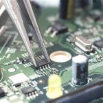
Manual placement involves using tweezers or a vacuum pen to pick up and place SMD components onto the PCB pads. This method is suitable for low-volume production, prototyping, or rework processes.
Tips for Manual SMD Component Placement
- Use appropriate tools, such as fine-tipped tweezers or a vacuum pen, to handle SMD components.
- Ensure proper lighting and magnification to accurately place components.
- Maintain a steady hand and use a light touch to avoid damaging components or disturbing solder paste.
- Double-check component orientation and alignment before soldering.
Automated SMD Component Placement
Automated placement using pick-and-place machines is the preferred method for high-volume production. These machines use computer-controlled nozzles to pick up SMD components from feeders and place them onto the PCB with high speed and precision.
Advantages of Automated SMD Component Placement
- High-speed placement, capable of placing thousands of components per hour
- Consistent and accurate placement, reducing the risk of human error
- Suitable for a wide range of component sizes and types
- Enables high-volume production and reduces labor costs
Challenges of Automated SMD Component Placement
- Requires significant investment in equipment and maintenance
- Programming and setup time for each PCB design
- Potential for machine downtime and maintenance issues

Solder Paste Selection and Application
Solder paste is a critical material in SMD welding, as it provides the means for creating a strong and reliable solder joint between the component leads and the PCB pads. Selecting the appropriate solder paste and applying it correctly are essential for successful SMD welding.
Solder Paste Composition
Solder paste is a homogeneous mixture of tiny solder particles (typically tin-lead or lead-free alloys) suspended in a flux medium. The flux helps to remove oxides, promote solder wetting, and protect the solder joint from oxidation during the welding process.
Solder Paste Selection Criteria
When selecting solder paste for SMD welding, consider the following factors:
- Alloy Composition: Choose a solder alloy that is compatible with the PCB and component materials, and meets the required melting temperature and strength properties.
- Particle Size: Select a solder paste with an appropriate particle size for the component pitch and PCB pad dimensions. Smaller particle sizes are suitable for fine-pitch components.
- Flux Type: Consider the flux type (rosin-based, water-soluble, or no-clean) based on the cleaning requirements and the PCB’s intended environment.
- Viscosity: Choose a solder paste viscosity that is suitable for the application method (stencil printing or dispensing) and ensures good print definition and release.
- Shelf Life: Ensure that the solder paste has an adequate shelf life and is stored under appropriate conditions to maintain its quality and performance.
Solder Paste Application Methods
There are two primary methods for applying solder paste in SMD welding: stencil printing and dispensing.
Stencil Printing
Stencil printing is the most common method for applying solder paste in high-volume production. It involves using a laser-cut or electroformed stencil with apertures that match the PCB pad layout. The stencil is placed over the PCB, and solder paste is deposited onto the pads using a squeegee or automated printer.
Dispensing
Dispensing is a selective solder paste application method suitable for low-volume production or rework processes. It involves using a pneumatic or positive displacement dispenser to apply solder paste directly onto specific PCB pads or components.
Inspection and Quality Control
Inspection and quality control are critical aspects of SMD welding to ensure the reliability and functionality of the final product. Various techniques are used to inspect and verify the quality of solder joints and detect potential defects.
Visual Inspection
Visual inspection is the most basic and widely used method for assessing the quality of SMD solder joints. It involves using the naked eye or magnification tools to examine the solder joints for defects such as bridging, insufficient solder, or poor wetting.
Automated Optical Inspection (AOI)
AOI is a computer-based inspection system that uses high-resolution cameras and image processing algorithms to detect solder joint defects automatically. AOI systems can quickly scan PCBs and identify issues such as missing components, misaligned components, or solder bridging.
X-Ray Inspection
X-ray inspection is used to examine solder joints that are hidden or obscured, such as those under Ball Grid Array (BGA) components. X-ray systems provide a non-destructive method for detecting solder joint defects, voids, or insufficient solder in areas that are not visible to the naked eye or AOI systems.
Electrical Testing
Electrical testing is performed to verify the functionality and performance of the assembled PCB. It involves using specialized equipment to test for short circuits, open circuits, or other electrical characteristics to ensure that the PCB meets the required specifications.
Best Practices for SMD Welding
To achieve consistent and reliable SMD welding results, consider the following best practices:
- Design for Manufacturability (DFM): Incorporate DFM principles during the PCB design stage to ensure compatibility with SMD welding processes, such as providing adequate pad sizes, spacing, and clearances.
- Component Selection: Choose SMD components that are suitable for the intended application, considering factors such as package size, thermal requirements, and compatibility with the welding process.
- Solder Paste Handling: Follow proper solder paste storage and handling guidelines to maintain its quality and performance, such as storing at the recommended temperature and using within the specified shelf life.
- Process Control: Implement strict process controls and monitor critical parameters such as reflow oven temperature profiles, solder paste print quality, and component placement accuracy to ensure consistent welding results.
- Cleanliness: Maintain a clean and contamination-free environment during SMD welding to prevent solder joint defects and ensure the long-term reliability of the assembled PCB.
- Training and Skill Development: Provide adequate training and skill development for operators involved in SMD welding processes to ensure adherence to best practices and minimize human errors.
Frequently Asked Questions (FAQ)
-
What is the difference between SMD and through-hole components?
SMD components are mounted directly onto the surface of the PCB, while through-hole components have leads that are inserted into holes drilled in the PCB and soldered on the opposite side. -
Can SMD components be soldered manually?
Yes, SMD components can be soldered manually using soldering irons and appropriate techniques. However, manual soldering is more suitable for low-volume production, prototyping, or rework processes. -
What is the purpose of flux in solder paste?
Flux in solder paste serves to remove oxides from the metal surfaces, promote solder wetting, and protect the solder joint from oxidation during the welding process. -
How can I prevent solder bridging in SMD welding?
To prevent solder bridging, ensure proper solder paste application, maintain appropriate solder paste viscosity, control the reflow oven temperature profile, and provide adequate spacing between components and pads in the PCB design. -
What are the advantages of lead-free solder in SMD welding?
Lead-free solder offers several advantages, including reduced environmental impact, compliance with RoHS regulations, and improved long-term reliability of solder joints. However, lead-free solder generally requires higher processing temperatures compared to leaded solder.
Conclusion
SMD welding is a vital process in modern electronics manufacturing, enabling the production of compact, high-performance, and cost-effective electronic devices. By understanding the various SMD welding techniques, component placement methods, solder paste selection and application, inspection and quality control measures, and best practices, manufacturers can optimize their SMD welding processes and ensure the reliability and functionality of their products.
As technology continues to advance, SMD welding processes will continue to evolve, with new materials, techniques, and automation solutions emerging to meet the ever-increasing demands of the electronics industry. By staying informed and adopting best practices, manufacturers can remain competitive and deliver high-quality products to their customers.
Leave a Reply