Introduction to Wave Soldering and PTH Components
Wave soldering is a widely used technique for soldering through-hole (PTH) components onto printed circuit boards (PCBs). It is an efficient and reliable method that has been in use for several decades in the electronics manufacturing industry. In this article, we will delve into the process of wave soldering, its advantages, and the key considerations when soldering PTH components.
What is Wave Soldering?
Wave soldering is a bulk soldering process where the PCB, with the components already inserted, is passed over a molten solder wave. The solder wave is created by a specialized machine that pumps molten solder through a nozzle, forming a standing wave. As the PCB comes into contact with the solder wave, the molten solder adheres to the component leads and the PCB’s through-holes, creating a strong electrical and mechanical connection.
What are PTH Components?
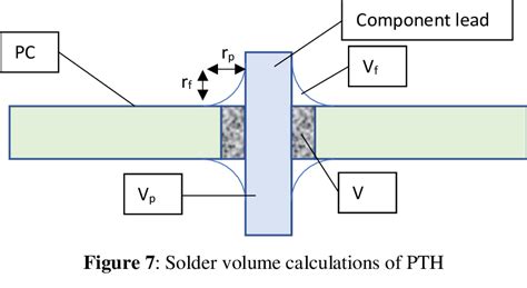
PTH (Plated Through-Hole) components are electronic components that have leads designed to be inserted into drilled holes on a PCB. These holes are typically plated with a conductive material, such as copper, to ensure a reliable electrical connection. PTH components include resistors, capacitors, inductors, connectors, and various other types of components commonly used in electronic assemblies.
Advantages of Wave Soldering for PTH Components
Wave soldering offers several advantages when it comes to soldering PTH components:
-
High Throughput: Wave soldering is a fast and efficient process that allows for the soldering of multiple components simultaneously. This makes it suitable for high-volume production, reducing the overall assembly time and cost.
-
Consistency: The automated nature of wave soldering ensures consistent solder joint quality across the entire PCB. The process parameters, such as solder temperature, conveyor speed, and flux application, can be precisely controlled, resulting in uniform and reliable solder connections.
-
Strong Mechanical Bonds: Wave soldering creates strong mechanical bonds between the component leads and the PCB. The molten solder flows into the through-holes and around the leads, forming a robust connection that can withstand mechanical stresses and vibrations.
-
Compatibility with Various Components: Wave soldering is compatible with a wide range of PTH components, including those with different lead sizes and shapes. It can handle components with long leads, such as connectors and switches, as well as smaller components like resistors and capacitors.
-
Cost-Effective: Compared to other soldering techniques, such as manual soldering or selective soldering, wave soldering is a cost-effective solution for high-volume production. The automated process reduces labor costs and minimizes the need for skilled operators.

Key Considerations for Wave Soldering PTH Components
To ensure successful wave soldering of PTH components, several key considerations must be taken into account:
1. PCB Design
The PCB design plays a crucial role in the success of wave soldering. Some important factors to consider include:
- Through-Hole Size: The diameter of the through-holes should be appropriate for the component leads. Oversized holes can lead to solder bridging, while undersized holes can cause insufficient solder fill.
- Pad Size: The pads surrounding the through-holes should be large enough to accommodate the solder fillet and provide adequate mechanical strength.
- Component Placement: Components should be placed with sufficient spacing to avoid solder bridging and allow for proper solder flow. Proper component orientation is also important to ensure correct polarity and prevent tombstoning.
2. Solder Mask and Pad Finish
The solder mask and pad finish on the PCB impact the wetting and flow of solder during wave soldering. A well-designed solder mask helps to prevent solder bridging and ensures that the solder only adheres to the desired areas. The pad finish, such as Hot Air Solder Leveling (HASL) or Electroless Nickel Immersion Gold (ENIG), affects the solderability and the final appearance of the solder joints.
3. Flux Selection and Application
Flux plays a critical role in wave soldering by removing oxides from the component leads and PCB pads, promoting solder wetting, and preventing re-oxidation during the soldering process. The selection of the appropriate flux depends on factors such as the type of PCB, component compatibility, and cleaning requirements. Flux can be applied using various methods, including foam fluxing, spray fluxing, or brush fluxing, depending on the specific requirements of the assembly.
4. Solder Alloy and Temperature
The choice of solder alloy and the operating temperature of the solder wave are important considerations. The most commonly used solder alloy for wave soldering is tin-lead (SnPb) solder, typically in the ratio of 63% tin and 37% lead. However, with the increasing demand for lead-free soldering, alternative alloys such as tin-silver-copper (SAC) are gaining popularity. The solder temperature should be carefully controlled to ensure proper melting and flow of the solder while avoiding component damage or PCB delamination.
5. Preheat and Cooling
Preheating the PCB and components before wave soldering is essential to minimize thermal shock and reduce the risk of component cracking or PCB warpage. The preheat temperature and duration should be optimized based on the PCB thickness, component thermal mass, and solder alloy used. After wave soldering, proper cooling of the PCB is necessary to allow the solder joints to solidify and prevent defects such as solder bridges or icicles.

Common Defects in Wave Soldering
Despite the advantages of wave soldering, certain defects can occur during the process. Some common defects include:
- Solder Bridges: Solder bridges are unintended connections between adjacent pads or leads caused by excessive solder. They can be prevented by proper PCB design, flux selection, and solder wave optimization.
- Insufficient Solder Fill: Insufficient solder fill occurs when the solder does not completely fill the through-holes or form a proper fillet around the component leads. This can be caused by inadequate preheat, low solder temperature, or poor wetting.
- Tombstoning: Tombstoning is a defect where a component stands up on one end due to uneven heating or solder surface tension. It can be minimized by proper component placement, preheat control, and solder wave design.
- Solder Balls: Solder balls are small spheres of solder that adhere to the PCB surface or component leads. They can be caused by excessive flux, contamination, or incorrect solder wave settings.
Regular inspection and quality control measures should be implemented to identify and address these defects promptly.

Frequently Asked Questions (FAQ)
-
Q: Can wave soldering be used for surface mount components?
A: While wave soldering is primarily used for PTH components, it can also be used for certain surface mount components with proper fixturing and process adjustments. However, for most surface mount components, reflow soldering is the preferred method. -
Q: Is wave soldering suitable for double-sided PCBs?
A: Yes, wave soldering can be used for double-sided PCBs. However, special considerations, such as the use of pallets or selective soldering, may be necessary to protect components on the top side of the PCB during the wave soldering process. -
Q: How does the conveyor speed affect the wave soldering process?
A: The conveyor speed determines the time the PCB spends in contact with the solder wave. A slower conveyor speed allows for better solder penetration and filling of through-holes but may increase the risk of heat damage to components. Conversely, a faster conveyor speed reduces the contact time but may result in insufficient solder fill. The optimal conveyor speed depends on factors such as the PCB thickness, component density, and solder alloy used. -
Q: What is the purpose of preheating in wave soldering?
A: Preheating serves several purposes in wave soldering. It activates the flux, removes moisture from the PCB and components, and reduces thermal shock when the PCB comes into contact with the molten solder. Preheating also helps to minimize component cracking, PCB warpage, and solder joint defects. -
Q: How often should the solder in the wave soldering machine be replaced?
A: The frequency of solder replacement depends on various factors, such as the volume of production, the quality of the solder, and the level of contamination. Regular monitoring of the solder quality, including visual inspection and chemical analysis, can help determine when the solder needs to be replaced. Generally, it is recommended to replace the solder when the contamination level exceeds the acceptable limits or when the solder composition deviates significantly from the desired specifications.
Conclusion
Wave soldering is a reliable and efficient method for soldering PTH components onto PCBs. It offers advantages such as high throughput, consistency, strong mechanical bonds, and cost-effectiveness. However, to achieve optimal results, careful consideration must be given to factors such as PCB design, solder mask and pad finish, flux selection, solder alloy and temperature, preheat and cooling, and defect prevention.
By understanding the key aspects of wave soldering and implementing best practices, manufacturers can ensure high-quality solder joints and reliable electronic assemblies. Regular process monitoring, quality control, and continuous improvement initiatives are essential to maintain the consistency and effectiveness of the wave soldering process.
As technology advances and new components and materials emerge, it is important for manufacturers to stay updated with the latest developments in wave soldering techniques and adapt their processes accordingly. By embracing innovation and adhering to industry standards, manufacturers can leverage the benefits of wave soldering to produce robust and reliable electronic products.


Leave a Reply