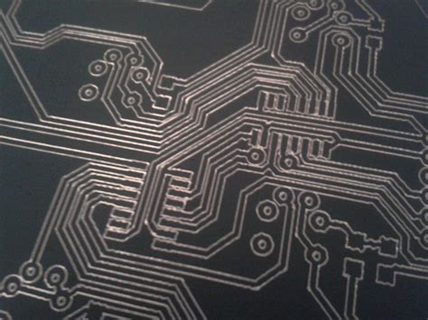
How laser cutting works for PCBs
The process of laser cutting PCBs involves using a high-powered laser to ablate and vaporize the unwanted copper from the surface of the PCB substrate material. The laser follows the paths defined in the PCB design file to selectively remove copper and electrically isolate the different traces and pads that form the circuit.
Some of the key advantages of laser cutting for PCB fabrication include:
- Extremely fine feature sizes and high precision (down to 25 microns)
- Fast processing speeds
- Low-cost setup and operation
- Environmentally friendly (no harsh chemicals needed)
- Works with a variety of PCB substrates
Types of lasers used
The two main types of lasers used for cutting PCBs are:
- CO2 lasers (10.6 μm wavelength)
- UV lasers (355 nm wavelength)
CO2 lasers are the most common and lowest cost option. They use an infrared beam to vaporize the copper. UV lasers have a shorter wavelength which allows for finer features and less thermal damage to the PCB substrate.
Here is a comparison of CO2 vs UV laser PCB cutting:
| Spec | CO2 laser | UV laser |
|---|---|---|
| Wavelength | 10.6 μm | 355 nm |
| Minimum feature size | 75 μm | 25 μm |
| Typical cutting speed | 200 mm/s | 100 mm/s |
| Thermal effect on PCB | 50-100 μm | 10-50 μm |
| Cost | $ | $$ |
Laser cut PCB materials
One of the benefits of laser cutting is that it works well with a variety of common PCB substrates, including:
- FR4 (standard)
- Aluminum
- Copper
- Polyimide
- Ceramics
The laser power and settings can be optimized based on the material properties to achieve the best quality cuts.
Designing PCBs for laser cutting
To take full advantage of laser cutting capabilities, there are some PCB design considerations to keep in mind:
Trace and space widths
Laser cutting allows for much finer trace widths and spacing compared to mechanical methods. Typical minimums are:
- 50 μm traces
- 50 μm spacing
Going below 50 μm is possible but will increase costs. The aspect ratio (depth:width) also becomes a limitation for narrow cuts.
Pad and hole sizes
The same applies for pad and hole sizes. Laser cutting enables smaller pads and holes but there are practical limits before costs increase:
- 200 μm min pad size
- 150 μm min hole size
Avoiding sharp angles
While laser cutting can do 90° angles, it’s best to avoid sharp angles in traces and pads. Adding fillets and chamfers allows the laser to change directions more smoothly which improves quality.
Minimizing stubs and loops
Stubs and loops of copper that aren’t connected to traces can cause issues with laser cutting. The isolated copper heats up and doesn’t get vaporized cleanly. It’s best to avoid these in your PCB design when possible.

Applications and use cases
Laser-cut PCBs are well-suited for a variety of electronics applications, especially those requiring:
- High density interconnects (HDI)
- Radio frequency (RF) circuits
- Embedded components
- Flexible or rigid-flex PCBs
Some example use cases include:
- Wearables and IoT devices
- Medical devices and sensors
- Aerospace and defense
- Automotive electronics
- LED lighting and displays

How to get started with laser-cut PCBs
If you’re interested in using laser-cut PCBs for your project, here are the typical steps:
- Create your PCB design using EDA or CAD software
- Generate the Gerber files or CAD drawing
- Request an online quote from a laser cutting PCB service
- Place your order and upload the design files
- Receive your custom laser-cut PCBs
There are a growing number of PCB manufacturers offering laser cutting services. Some popular online services include:
- PCBWay
- OSH Park
- Pad2Pad
- Accutrace
Lead times are typically 1-2 weeks but rush production is often available. Costs depend on the PCB specs but can be as low as $1 per board.

Frequently Asked Questions
How much do laser cut PCBs cost?
Costs for laser-cut PCBs depend on the number of boards, size, number of layers, materials, and features. In general, prices start around $1 per board for small quantities. Larger quantities and more complex designs will cost more but are still very competitive with traditional PCB pricing.
What are the advantages of laser cutting vs other PCB methods?
The main advantages of laser cutting over methods like mechanical milling or chemical etching are:
- Faster production times
- No hard tooling costs
- Finer resolution and smaller features
- More environmentally friendly
- Works with a wider variety of materials
How small of features can laser cutting produce?
With UV lasers and optimized settings, the minimum feature sizes are:
- 25 μm trace and space widths
- 75 μm pad and hole sizes
Achieving these minimums may increase costs. More typical minimums are 50 μm traces and 150 μm holes.
How thick of copper can be laser cut?
Standard 1 oz copper (~35 μm thick) is not a problem for laser cutting. 2 oz and even 4 oz copper can also be cut but will be slower. The aspect ratio of copper thickness to minimum feature size can become a limitation for heavier copper weights.
What file formats are needed for laser cutting PCBs?
The standard file formats used for laser-cut PCBs are:
- Gerber (RS-274X)
- Excellon drill
- ODB++
- AutoCAD DXF
Most PCB design software can export these formats. The exact file requirements may vary by manufacturer, so be sure to check their guidelines.
Conclusion
Laser cutting is a powerful and increasingly accessible technology for PCB fabrication. It offers several advantages over traditional manufacturing methods in terms of speed, cost, resolution, and material flexibility.
As laser cutting continues to advance, it will enable even more complex and innovative PCB designs. From IoT devices to advanced medical sensors, laser-cut PCBs are helping to push the boundaries of what’s possible in electronics.
If you’re looking for a fast, affordable, and high-precision way to prototype or produce PCBs, laser cutting is definitely worth considering for your next project.


Leave a Reply