Introduction to LPI Soldermask and Silk Screen Printing
Liquid photoimageable (LPI) soldermask is a crucial component in the production of printed circuit boards (PCBs). It serves as a protective layer that covers the copper traces on the PCB, preventing oxidation and providing electrical insulation. Additionally, soldermask improves the PCB’s aesthetics and enhances the accuracy of the soldering process by defining the areas where solder should be applied.
Among the various methods of applying LPI soldermask, silk screen printing is the most widely used technique in the PCB industry. This article will delve into the details of LPI soldermask, the silk screen printing process, its advantages, and its role in the PCB manufacturing process.
What is LPI Soldermask?
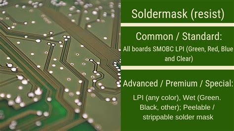
LPI soldermask is a photoimageable polymer coating that is applied to the surface of a PCB. It is typically green in color but can also be found in other colors such as red, blue, yellow, black, and white. The primary functions of LPI soldermask are:
- Protection: It shields the copper traces from oxidation, scratches, and other environmental factors that can damage the PCB.
- Insulation: LPI soldermask provides electrical insulation between the copper traces, preventing short circuits and ensuring the proper functioning of the PCB.
- Solder Control: It defines the areas where solder should be applied during the soldering process, improving the accuracy and reliability of the solder joints.
- Aesthetics: LPI soldermask gives the PCB a professional and appealing appearance, which is particularly important for consumer electronics.
Advantages of LPI Soldermask
LPI soldermask offers several advantages over other types of soldermask, such as dry film soldermask and liquid soldermask:
- High Resolution: LPI soldermask can achieve finer feature sizes and higher resolution compared to other soldermask types, making it suitable for high-density PCB designs.
- Excellent Adhesion: It forms a strong bond with the PCB surface, ensuring long-term protection and durability.
- Flexibility: LPI soldermask has good flexibility, allowing it to withstand the stresses caused by thermal expansion and contraction during the PCB’s operation.
- Chemical Resistance: It is resistant to a wide range of chemicals, including acids, alkalis, and solvents, which helps maintain the PCB’s integrity in harsh environments.
The Silk Screen Printing Process for LPI Soldermask Application
Silk screen printing is a stencil-based printing technique that involves forcing the LPI soldermask through a fine mesh screen onto the PCB surface. The process consists of several steps, which are outlined below:
Step 1: Screen Preparation
The first step in the silk screen printing process is to create a stencil of the desired soldermask pattern on a fine mesh screen. The screen is typically made of polyester or stainless steel, with a mesh count ranging from 80 to 400 threads per inch. A photosensitive emulsion is applied to the screen and then exposed to UV light through a film positive of the soldermask artwork. The unexposed areas of the emulsion are washed away, leaving behind a stencil of the soldermask pattern.
Step 2: PCB Preparation
Before applying the LPI soldermask, the PCB surface must be cleaned and treated to ensure proper adhesion. This typically involves the following sub-steps:
- Cleaning: The PCB is cleaned using a mild detergent or a specialized PCB cleaner to remove any dirt, grease, or contaminants from the surface.
- Microetching: A microetch solution is applied to the PCB to roughen the copper surface slightly, promoting better adhesion of the soldermask.
- Pre-baking: The PCB is baked in an oven at a temperature of around 150°C for 30-60 minutes to remove any moisture and improve adhesion.
Step 3: Soldermask Application
With the screen and PCB prepared, the LPI soldermask is applied using the silk screen printing process:
- Alignment: The PCB is aligned with the soldermask screen using registration marks to ensure accurate placement of the soldermask pattern.
- Printing: The LPI soldermask is dispensed onto the screen and then forced through the mesh openings using a squeegee. The soldermask is deposited onto the PCB surface in the desired pattern.
- Inspection: After printing, the PCB is inspected for any defects or irregularities in the soldermask application, such as pinholes, bubbles, or insufficient coverage.
Step 4: Curing
After the LPI soldermask is applied, it must be cured to cross-link the polymer and form a stable, protective layer. The curing process involves two stages:
- Pre-curing: The PCB is exposed to UV light for a short duration (typically 30-60 seconds) to partially cure the soldermask and make it more manageable for handling.
- Final Curing: The PCB is then baked in an oven at a temperature of around 150°C for 30-60 minutes to fully cure the soldermask and achieve its final properties.
Step 5: Final Inspection and Testing
After curing, the PCB undergoes a final visual inspection to ensure that the soldermask application is free of defects and meets the required specifications. Electrical testing may also be performed to verify the PCB’s functionality and the soldermask’s insulating properties.

Advantages of Silk Screen Printing for LPI Soldermask Application
Silk screen printing offers several advantages for the application of LPI soldermask:
- Cost-Effective: Silk screen printing is a relatively inexpensive process compared to other soldermask application methods, making it suitable for high-volume production.
- High Throughput: The process is fast and efficient, allowing for the rapid application of soldermask to a large number of PCBs.
- Consistency: Silk screen printing produces consistent results, ensuring uniform coverage and thickness of the soldermask across the PCB surface.
- Versatility: The process can be used for a wide range of PCB sizes and shapes, and it can accommodate various soldermask formulations.

Factors Affecting the Quality of Silk Screen Printed LPI Soldermask
Several factors can influence the quality of the silk screen printed LPI soldermask:
- Screen Mesh Count: The mesh count of the screen determines the resolution and thickness of the soldermask application. Higher mesh counts produce finer features but may result in a thinner soldermask layer.
- Emulsion Thickness: The thickness of the photosensitive emulsion on the screen affects the depth of the stencil and, consequently, the thickness of the applied soldermask.
- Squeegee Pressure and Speed: The pressure applied by the squeegee and the speed at which it is moved across the screen can impact the uniformity and coverage of the soldermask.
- Soldermask Viscosity: The viscosity of the LPI soldermask must be carefully controlled to ensure proper flow through the screen and adequate coverage on the PCB surface.
- Curing Parameters: The UV exposure time and oven baking temperature and duration must be optimized to achieve complete curing of the soldermask without causing any damage to the PCB.

Comparison of Silk Screen Printing with Other LPI Soldermask Application Methods
While silk screen printing is the most common method for applying LPI soldermask, there are other techniques available, such as curtain coating, spray coating, and inkjet printing. The following table compares these methods based on various factors:
| Factor | Silk Screen Printing | Curtain Coating | Spray Coating | Inkjet Printing |
|---|---|---|---|---|
| Cost | Low to Medium | Medium to High | Medium | High |
| Throughput | High | High | Medium | Low to Medium |
| Resolution | High | Medium | Medium | Very High |
| Thickness Control | Good | Excellent | Good | Excellent |
| Soldermask Utilization | Moderate | High | Moderate | High |
| Equipment Complexity | Low to Medium | High | Medium | High |
| Maintenance Requirements | Low to Medium | High | Medium | High |
As evident from the table, each method has its strengths and weaknesses. The choice of the LPI soldermask application method depends on factors such as the PCB design complexity, production volume, cost considerations, and the available equipment and expertise.
FAQ
1. What is the typical thickness of LPI soldermask applied using silk screen printing?
The typical thickness of LPI soldermask applied using silk screen printing ranges from 10 to 50 microns (0.4 to 2 mils). The exact thickness depends on factors such as the screen mesh count, emulsion thickness, and soldermask viscosity.
2. Can silk screen printing be used for applying soldermask to both sides of the PCB?
Yes, silk screen printing can be used to apply soldermask to both sides of the PCB. This is typically done in two separate printing stages, with the PCB being flipped over after the first side is printed and cured.
3. How does the color of the LPI soldermask affect its performance?
The color of the LPI soldermask does not significantly affect its performance in terms of protection, insulation, or solder control. However, some colors may have slightly different curing requirements or may be more susceptible to UV degradation over time.
4. What is the shelf life of LPI soldermask used in silk screen printing?
The shelf life of LPI soldermask depends on the specific formulation and storage conditions. Most LPI soldermasks have a shelf life of 6 to 12 months when stored in a cool, dry place away from direct sunlight. It is important to follow the manufacturer’s storage and handling guidelines to ensure optimal performance.
5. Can silk screen printing be used for applying soldermask to flexible PCBs?
Yes, silk screen printing can be used for applying soldermask to flexible PCBs. However, the process may require some modifications, such as using a more flexible screen material and adjusting the curing parameters to account for the different substrate properties. It is essential to work closely with the PCB fabricator and soldermask supplier to ensure compatibility and optimal results.
Conclusion
Silk screen printing is the most widely used method for applying LPI soldermask in the PCB industry. Its cost-effectiveness, high throughput, consistency, and versatility make it an attractive choice for PCB manufacturers. By understanding the silk screen printing process, its advantages, and the factors affecting the quality of the soldermask application, PCB designers and manufacturers can ensure the production of high-quality, reliable, and visually appealing PCBs.
As PCB designs continue to evolve and become more complex, the importance of effective and efficient LPI soldermask application methods will only grow. Silk screen printing, with its proven track record and adaptability, is well-positioned to meet the ever-changing demands of the PCB industry.


Leave a Reply