What is LPI Solder Mask?
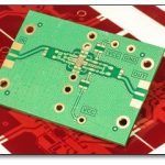
LPI solder mask is a photosensitive polymer coating that is applied to the surface of a PCB. It is designed to selectively expose and cure when subjected to ultraviolet (UV) light, creating a permanent protective layer on the PCB. The LPI solder mask is typically green in color, although other colors such as red, blue, and black are also available to meet specific design requirements.
The composition of LPI solder mask includes:
- Photosensitive resins
- Fillers
- Pigments
- Additives
These components work together to provide the desired properties, such as excellent adhesion, high resolution, and resistance to chemicals and heat.
Advantages of LPI Solder Mask
LPI solder mask offers several advantages over traditional solder mask application methods, such as screen printing and dry film solder mask. Some of the key benefits include:
-
Higher resolution: LPI solder mask can achieve finer feature sizes and more precise registration, enabling the creation of high-density PCBs with smaller pitch sizes.
-
Improved uniformity: The liquid nature of LPI solder mask allows for a more even and consistent coating across the PCB surface, reducing the risk of defects and ensuring better performance.
-
Enhanced adhesion: LPI solder mask exhibits excellent adhesion to the copper traces and laminate, minimizing the chances of delamination or lifting during the assembly process.
-
Increased efficiency: The LPI solder mask application process is highly automated, reducing manual labor and improving overall production efficiency.
LPI Solder Mask Application Process
The LPI solder mask application process involves several steps, each of which is critical to ensuring a high-quality finish. The main stages of the process are as follows:
1. Surface Preparation
Before applying the LPI solder mask, the PCB surface must be thoroughly cleaned and prepared. This involves removing any contaminants, such as dirt, grease, or oxidation, that may interfere with the adhesion of the solder mask. The cleaning process typically includes the following steps:
- Degreasing: The PCB is immersed in a degreasing solution to remove oils and grease from the surface.
- Microetching: A mild etching solution is used to roughen the copper surface, promoting better adhesion of the solder mask.
- Rinsing: The PCB is rinsed with water to remove any residual chemicals and debris.
- Drying: The PCB is dried using hot air or an oven to ensure a moisture-free surface.
2. LPI Solder Mask Coating
Once the PCB surface is prepared, the LPI solder mask is applied using a coating machine. There are two primary methods for LPI solder mask coating:
Curtain Coating
In the curtain coating process, the LPI solder mask is dispensed in a continuous curtain across the width of the PCB. The PCB is passed through the curtain at a controlled speed, ensuring an even and uniform coating. Curtain coating is suitable for high-volume production and can achieve coating thicknesses ranging from 15 to 50 microns.
Advantages of curtain coating include:
- High throughput
- Consistent coating thickness
- Minimal waste
Spray Coating
Spray coating involves atomizing the LPI solder mask into fine droplets and spraying it onto the PCB surface using a spray nozzle. The PCB is typically placed on a conveyor belt that moves at a controlled speed beneath the spray nozzle. Spray coating offers greater flexibility in terms of coating thickness and can accommodate PCBs with complex geometries.
Advantages of spray coating include:
- Adjustable coating thickness
- Ability to coat irregularly shaped PCBs
- Reduced material consumption
After the LPI solder mask is applied, the PCB undergoes a pre-drying process to remove excess solvent and stabilize the coating. Pre-drying is typically carried out in a convection oven at temperatures ranging from 70 to 90°C for 15 to 30 minutes.
3. Exposure
The next step in the LPI solder mask application process is exposure. The coated PCB is aligned with a photomask, which contains the desired solder mask pattern. The photomask is typically made of glass or film and has clear and opaque areas corresponding to the areas where the solder mask should be removed or retained.
The aligned PCB and photomask are then exposed to UV light using an exposure machine. The UV light passes through the clear areas of the photomask and polymerizes the LPI solder mask in those regions, making it resistant to the subsequent developing process. The exposure time and intensity depend on factors such as the solder mask thickness, the type of UV light source, and the desired resolution.
4. Developing
After exposure, the PCB undergoes a developing process to remove the unexposed areas of the LPI solder mask. The developing solution, typically an alkaline solution, selectively dissolves the non-polymerized solder mask, leaving behind the desired pattern.
The developing process involves the following steps:
-
Immersion: The PCB is immersed in the developing solution for a specified time, usually ranging from 60 to 180 seconds, depending on the solder mask thickness and the desired resolution.
-
Spraying: The PCB is then sprayed with a pressurized stream of the developing solution to remove any remaining unexposed solder mask.
-
Rinsing: The PCB is rinsed with water to remove the developing solution and any dissolved solder mask.
-
Drying: The PCB is dried using hot air or an oven to remove any residual moisture.
5. Final Curing
After developing, the PCB undergoes a final curing process to fully polymerize and harden the LPI solder mask. The curing process is typically carried out in a convection oven at temperatures ranging from 140 to 160°C for 60 to 90 minutes. The high temperature ensures complete cross-linking of the polymer chains, resulting in a durable and resistant solder mask layer.

LPI Solder Mask Performance Requirements
To ensure the quality and reliability of the LPI solder mask, several performance requirements must be met. These requirements are outlined in industry standards such as IPC-SM-840 and IPC-A-600. Some of the key performance criteria include:
-
Adhesion: The LPI solder mask must exhibit excellent adhesion to the PCB surface, withstanding the stresses encountered during the assembly process and throughout the product life cycle. Adhesion is typically tested using the cross-hatch test method (IPC-TM-650 2.4.1).
-
Resistance to chemicals: The LPI solder mask should be resistant to a variety of chemicals used in the PCB assembly process, such as fluxes, solvents, and cleaning agents. Chemical resistance is evaluated using the solvent resistance test (IPC-TM-650 2.3.2) and the flux resistance test (IPC-TM-650 2.6.3.7).
-
Thermal resistance: The LPI solder mask must withstand the high temperatures encountered during soldering and other thermal processes without degrading or losing its protective properties. Thermal resistance is assessed using the solder float test (IPC-TM-650 2.6.8) and the thermal shock test (IPC-TM-650 2.6.7.1).
-
Electrical insulation: The LPI solder mask should provide adequate electrical insulation between adjacent conductive elements on the PCB. Insulation properties are evaluated using the dielectric withstanding voltage test (IPC-TM-650 2.5.7) and the insulation resistance test (IPC-TM-650 2.6.3.1).
-
Resolution and registration: The LPI solder mask must be capable of achieving fine feature sizes and precise registration to ensure proper coverage of the desired areas on the PCB. Resolution and registration are assessed using visual inspection and microscopic examination.
Troubleshooting and Defect Prevention
Despite the advanced technologies and processes used in LPI solder mask application, defects can still occur. Some common LPI solder mask defects include:
- Pinholes: Small, circular openings in the solder mask that expose the underlying copper.
- Solder mask bridge: Unintended connection of solder mask between adjacent pads or traces.
- Solder mask residue: Incomplete removal of unexposed solder mask during the developing process.
- Misregistration: Misalignment of the solder mask pattern with respect to the copper features.
To minimize the occurrence of these defects, it is essential to implement proper process controls and adhere to best practices. Some strategies for defect prevention include:
-
Maintaining a clean and contaminant-free environment throughout the LPI solder mask application process.
-
Regularly calibrating and maintaining the coating, exposure, and developing equipment to ensure consistent performance.
-
Using high-quality LPI solder mask materials and photomasks that meet the required specifications.
-
Implementing statistical process control (SPC) methods to monitor key process parameters and identify potential issues before they result in defects.
-
Conducting thorough visual inspections and electrical testing to detect and address any defects before the PCBs proceed to the next stage of production.
Frequently Asked Questions (FAQ)
1. What is the typical thickness of LPI solder mask?
The typical thickness of LPI solder mask ranges from 15 to 50 microns, depending on the application method and the specific requirements of the PCB. Curtain coating generally results in thicker coatings, while spray coating allows for more precise control over the thickness.
2. Can LPI solder mask be applied to flexible PCBs?
Yes, LPI solder mask can be applied to flexible PCBs, although the process may require some modifications to accommodate the unique characteristics of flexible substrates. Special formulations of LPI solder mask, such as those with increased flexibility and elongation, are often used for flexible PCB applications.
3. How does LPI solder mask compare to other solder mask types, such as dry film and screen-printed solder mask?
LPI solder mask offers several advantages over dry film and screen-printed solder mask, including higher resolution, better uniformity, and improved adhesion. However, LPI solder mask application requires more specialized equipment and processes, which can increase production costs compared to other methods.
4. What is the shelf life of LPI solder mask, and how should it be stored?
The shelf life of LPI solder mask varies depending on the specific product and storage conditions. Most LPI solder mask formulations have a shelf life of 6 to 12 months when stored in a cool, dry place away from direct sunlight. It is essential to follow the manufacturer’s storage recommendations to ensure optimal performance.
5. Can LPI solder mask be reworked or repaired if defects are detected after application?
In some cases, LPI solder mask defects can be reworked or repaired, depending on the nature and extent of the defect. Minor defects, such as small pinholes or solder mask residue, can often be corrected using touch-up methods or selective removal techniques. However, more severe defects, such as large-scale misregistration or delamination, may require stripping and reapplying the solder mask entirely.
LPI Solder Mask Application Equipment
The equipment used for LPI solder mask application plays a crucial role in ensuring a high-quality finish and efficient production process. Some of the key equipment components include:
| Equipment | Function |
|---|---|
| Coating machine | Applies the LPI solder mask to the PCB surface using curtain coating or spray coating methods. |
| Pre-drying oven | Removes excess solvent and stabilizes the LPI solder mask coating before exposure. |
| Exposure machine | Aligns the coated PCB with the photomask and exposes it to UV light to polymerize the desired solder mask pattern. |
| Developing machine | Removes the unexposed areas of the LPI solder mask using a developing solution and spraying process. |
| Final curing oven | Fully polymerizes and hardens the LPI solder mask through a high-temperature curing process. |
| Automated optical inspection (AOI) system | Performs automated visual inspection of the applied solder mask to detect defects and ensure conformance to specifications. |
Investing in high-quality equipment and regular maintenance is essential for achieving consistent and reliable LPI solder mask application results.
Conclusion
LPI solder mask application is a critical process in the manufacturing of high-quality PCBs. By providing a protective layer on the PCB surface, LPI solder mask ensures the reliability and performance of the final product. The LPI solder mask application process involves several key steps, including surface preparation, coating, exposure, developing, and final curing.
To achieve the best results, it is essential to follow best practices, implement proper process controls, and invest in high-quality equipment and materials. By understanding the principles and techniques behind LPI solder mask application, PCB manufacturers can optimize their processes, minimize defects, and produce PCBs that meet the ever-increasing demands of the electronics industry.
As technology continues to advance, the importance of LPI solder mask application will only grow. By staying up-to-date with the latest developments and continuously improving their processes, PCB manufacturers can remain competitive and deliver the high-quality products that their customers require.

Leave a Reply