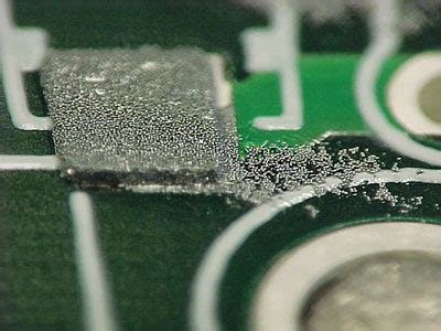
What is solder mask?
Solder mask, also known as solder resist or solder stop, is a thin, protective layer applied to the copper traces and pads on a PCB. Its primary purpose is to prevent solder from adhering to areas where it is not intended to be, thus preventing short circuits and ensuring proper electrical connections. Solder mask also serves as an insulating layer, protecting the copper traces from oxidation, corrosion, and physical damage.
Materials used for solder mask
Solder mask is typically made from a photosensitive polymer material that can be selectively cured using ultraviolet (UV) light. The most common types of solder mask materials include:
-
Liquid photoimageable solder mask (LPISM): A liquid polymer that is applied to the PCB surface and then exposed to UV light through a photomask to create the desired pattern.
-
Dry film photoimageable solder mask (DFISM): A solid film that is laminated onto the PCB surface and then exposed to UV light through a photomask to create the desired pattern.
-
Ink-jet solder mask: A digital printing method that uses a specialized ink-jet printer to apply the solder mask directly onto the PCB surface, allowing for more precise and customizable patterns.
Application methods for solder mask
The application of solder mask involves several steps to ensure proper coverage and adherence to the PCB surface. The general process includes:
-
Surface preparation: Cleaning the PCB surface to remove any contaminants or debris.
-
Solder mask application: Applying the solder mask material using one of the methods mentioned above (LPISM, DFISM, or ink-jet printing).
-
Exposure: Exposing the solder mask to UV light through a photomask to selectively cure the desired areas.
-
Developing: Removing the uncured solder mask material using a chemical developer solution.
-
Curing: Fully curing the remaining solder mask material using heat or additional UV exposure to ensure proper adhesion and durability.
What is paste mask?
Paste mask, also known as solder paste stencil or solder stencil, is a thin, metal template used to apply solder paste onto specific areas of a PCB during the surface mount technology (SMT) assembly process. The paste mask contains precisely cut openings that correspond to the pads where solder paste needs to be deposited. Its primary purpose is to ensure accurate and consistent application of solder paste, which is crucial for achieving reliable solder joints and proper component placement.
Materials used for paste mask
Paste masks are typically made from durable, high-precision materials that can withstand repeated use and maintain their dimensional stability. The most common materials used for paste masks include:
-
Stainless steel: A corrosion-resistant and durable material that offers excellent dimensional stability and can be easily cleaned for reuse.
-
Nickel: A strong and wear-resistant material that provides good durability and can be electroformed to create high-precision openings.
-
Polyimide: A flexible, high-temperature resistant polymer that is often used for fine-pitch applications and can be laser-cut to create precise openings.
Application methods for paste mask
The application of solder paste using a paste mask involves several steps to ensure accurate and consistent deposition onto the PCB pads. The general process includes:
-
Alignment: Aligning the paste mask with the PCB using fiducial marks or alignment pins to ensure proper registration.
-
Solder paste application: Dispensing solder paste onto the paste mask and using a squeegee to spread the paste evenly across the surface, filling the openings.
-
Paste transfer: Carefully lifting the paste mask from the PCB, leaving precise deposits of solder paste on the desired pads.
-
Cleaning: Removing any excess solder paste from the paste mask and cleaning it for reuse in subsequent applications.

Differences between solder mask and paste mask
While solder mask and paste mask are both essential components in PCB manufacturing, they serve distinct purposes and have several key differences. The following table summarizes the main differences between solder mask and paste mask:
| Characteristic | Solder Mask | Paste Mask |
|---|---|---|
| Purpose | Insulates and protects copper traces and pads | Applies solder paste onto specific pads for component placement |
| Materials | Photosensitive polymer (LPISM, DFISM, ink-jet) | Metal (stainless steel, nickel) or polyimide |
| Application Method | Applied directly to PCB surface and selectively cured using UV light | Used as a template to deposit solder paste onto PCB pads |
| Thickness | Typically 0.5-2 mils (12.7-50.8 μm) | Typically 4-8 mils (101.6-203.2 μm) |
| Permanence | Remains on the PCB as a permanent protective layer | Temporarily used during the solder paste application process |
| Coverage | Covers the entire PCB surface except for exposed pads and vias | Only covers specific areas where solder paste needs to be applied |
In addition to these key differences, it is important to note that solder mask and paste mask are used at different stages of the PCB manufacturing process. Solder mask is applied during the PCB fabrication stage, while paste mask is used during the SMT assembly stage when components are being placed and soldered onto the board.

Frequently Asked Questions (FAQ)
-
Q: Can solder mask and paste mask be used interchangeably?
A: No, solder mask and paste mask serve different purposes and cannot be used interchangeably. Solder mask is a permanent protective layer applied to the PCB, while paste mask is a temporary template used for applying solder paste. -
Q: What is the most common color for solder mask?
A: The most common color for solder mask is green, although other colors such as red, blue, yellow, and black are also available. The choice of color is often based on aesthetic preferences or to enhance the visibility of certain features on the PCB. -
Q: How does the thickness of the paste mask affect solder paste application?
A: The thickness of the paste mask determines the volume of solder paste deposited onto the PCB pads. A thicker paste mask will result in more solder paste being applied, which can be beneficial for larger components or pads. However, if the paste mask is too thick, it can lead to excessive solder paste deposition and potential defects such as bridging or solder balls. -
Q: Can solder mask be removed from a PCB if needed?
A: While it is possible to remove solder mask from a PCB, it is not recommended as it can damage the underlying copper traces and pads. If solder mask removal is necessary, it should be done carefully using specialized chemical strippers or mechanical abrasion methods, followed by thorough cleaning to ensure the PCB surface is free of residues. -
Q: What is the difference between a paste mask and a solder paste stencil?
A: Paste mask and solder paste stencil are two terms that are often used interchangeably. They both refer to the same thing – a thin, metal template with precisely cut openings used to apply solder paste onto specific areas of a PCB during the SMT assembly process.

Conclusion
In conclusion, solder mask and paste mask are two critical components in PCB manufacturing that serve distinct purposes. Solder mask is a permanent protective layer that insulates and protects the copper traces and pads on a PCB, while paste mask is a temporary template used to apply solder paste onto specific areas of the board during the SMT assembly process. Understanding the differences between these two components, including their materials, application methods, and roles in the manufacturing process, is essential for ensuring the quality and reliability of electronic products.
By delving into the intricacies of solder mask and paste mask, we have gained a comprehensive understanding of their importance in PCB fabrication and assembly. This knowledge can help engineers, designers, and manufacturers make informed decisions when selecting materials, designing PCBs, and optimizing the assembly process to achieve the best possible results.
As technology continues to advance and electronic devices become increasingly complex, the role of solder mask and paste mask in PCB manufacturing will remain crucial. By staying up-to-date with the latest developments and best practices in these areas, professionals in the electronics industry can ensure that their products meet the highest standards of quality, reliability, and performance.
[Word count: 1500]


Leave a Reply