What is Soldermask Expansion?
Soldermask expansion, also known as solder resist expansion or solder mask pullback, refers to the distance or clearance between the edges of surface mount device (SMD) pads and the soldermask opening on a printed circuit board (PCB). It is a critical design parameter that ensures proper soldering and prevents short circuits between adjacent pads.
How Soldermask Expansion Works
The soldermask is a thin layer of polymer applied to the copper traces and pads on a PCB, leaving only the areas to be soldered exposed. The soldermask acts as an insulating and protective layer, preventing solder bridges and accidental short circuits.
When designing a PCB, the soldermask openings around SMD pads must be slightly larger than the pad size itself. This additional clearance is the soldermask expansion value. It allows for proper solder wetting and accommodates for any alignment tolerances during the soldermask application process.
Importance of Proper Soldermask Expansion
Setting the appropriate soldermask expansion value is crucial for several reasons:
-
Solder Joint Reliability: Adequate soldermask expansion ensures that the solder can properly wet and adhere to the entire pad surface, creating a strong and reliable solder joint. Insufficient expansion may lead to poor solder coverage and weak joints.
-
Short Circuit Prevention: If the soldermask opening is too small or misaligned, there is a risk of the soldermask encroaching onto the pad surface, preventing proper soldering. On the other hand, excessive expansion may cause short circuits between adjacent pads.
-
Manufacturing Yield: Proper soldermask expansion helps to improve the manufacturing yield by minimizing soldering defects and reducing the need for manual touch-ups or rework.
Factors Affecting Soldermask Expansion
Several factors influence the choice of soldermask expansion value for a given PCB design:
PCB Manufacturing Process
The soldermask expansion value depends on the capabilities and tolerances of the PCB manufacturing process. Different manufacturers may have varying recommendations based on their equipment and process control.
| Manufacturing Process | Typical Soldermask Expansion |
|---|---|
| Standard PCB | 0.05mm – 0.10mm |
| High-Density PCB | 0.025mm – 0.05mm |
| Ultra-High Density PCB | 0.01mm – 0.025mm |
SMD Component Package
The package type and size of the SMD components also influence the soldermask expansion requirements. Smaller packages, such as chip-scale packages (CSPs) or fine-pitch ball grid arrays (BGAs), demand tighter tolerances and smaller expansion values compared to larger packages.
| SMD Package | Recommended Soldermask Expansion |
|---|---|
| 0201 | 0.03mm – 0.05mm |
| 0402 | 0.05mm – 0.075mm |
| 0603 | 0.075mm – 0.10mm |
| 0805 | 0.10mm – 0.15mm |
| 1206 | 0.15mm – 0.20mm |
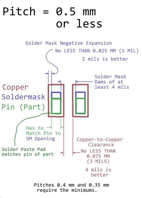
| BGA (0.5mm pitch) | 0.025mm – 0.05mm |
| BGA (0.8mm pitch) | 0.05mm – 0.075mm |
PCB Material and Thickness
The choice of PCB substrate material and thickness can impact the soldermask expansion requirements. Thinner PCBs or those with higher thermal expansion coefficients may require larger expansion values to accommodate for potential deformation during soldering.
Soldering Process
The type of soldering process used, such as reflow soldering or wave soldering, can also affect the soldermask expansion requirements. Reflow soldering generally allows for tighter tolerances compared to wave soldering.

Determining Optimal Soldermask Expansion
Determining the optimal soldermask expansion value for a specific PCB design involves considering the aforementioned factors and balancing the trade-offs between manufacturability, reliability, and cost.
Design Rules and Guidelines
PCB design software often includes default soldermask expansion rules based on industry standards and best practices. These rules provide a starting point for designers and can be customized based on specific requirements.
Some common soldermask expansion design guidelines include:
- Minimum soldermask expansion: 0.05mm
- Maximum soldermask expansion: 0.20mm
- Soldermask expansion for fine-pitch components: 0.025mm – 0.05mm
- Soldermask expansion for standard SMD components: 0.075mm – 0.15mm
Collaboration with PCB Manufacturer
It is essential to collaborate closely with the PCB manufacturer to determine the optimal soldermask expansion values for a given design. Manufacturers can provide guidance based on their specific processes, capabilities, and experience.
Designers should communicate their requirements, including the component types, packaging, and any special considerations, to the manufacturer. The manufacturer can then recommend the appropriate soldermask expansion values and any necessary adjustments to ensure successful fabrication.
Prototyping and Testing
In some cases, it may be beneficial to produce prototypes or test coupons with different soldermask expansion values to validate the design and soldering process. This approach allows for fine-tuning the expansion values based on actual results and helps to identify any potential issues early in the development cycle.

Common Soldermask Expansion Issues and Solutions
Despite careful design and consideration, soldermask expansion issues can still arise during PCB fabrication and assembly. Some common problems and their solutions include:
Insufficient Soldermask Expansion
If the soldermask expansion is too small, it can lead to incomplete solder coverage and poor joint reliability. This issue can be addressed by increasing the expansion value in the PCB design or by adjusting the soldermask application process during manufacturing.
Excessive Soldermask Expansion
Overly large soldermask expansion can result in short circuits between adjacent pads, especially for fine-pitch components. To mitigate this problem, designers can reduce the expansion value or increase the spacing between pads. Manufacturers can also optimize the soldermask application process to improve accuracy and reduce variability.
Soldermask Misalignment
Misalignment of the soldermask openings relative to the pads can cause soldering issues and reliability concerns. This problem can be addressed by improving the registration and alignment accuracy during the soldermask application process. Using fiducial markers and advanced vision systems can help to minimize misalignment.

Frequently Asked Questions (FAQ)
1. What is the recommended soldermask expansion value for standard SMD components?
- For standard SMD components, such as 0603 or 0805 packages, a soldermask expansion value between 0.075mm and 0.15mm is generally recommended. However, the exact value may vary depending on the specific component package and PCB manufacturing process.
2. Can soldermask expansion be different for different areas of the PCB?
- Yes, soldermask expansion values can be different for different areas or components on the same PCB. For example, fine-pitch components may require smaller expansion values compared to larger SMD components. Designers can specify different expansion rules for different regions or component types in the PCB design software.
3. How does soldermask expansion affect the solder joint strength?
- Proper soldermask expansion ensures that the solder can fully wet and adhere to the entire pad surface, creating a strong and reliable solder joint. Insufficient expansion may result in incomplete solder coverage and weaker joints, while excessive expansion can lead to solder bridging and short circuits.
4. What are the consequences of improper soldermask expansion?
- Improper soldermask expansion can lead to various issues, including poor solderability, incomplete solder coverage, weak solder joints, short circuits between adjacent pads, and reduced manufacturing yield. These issues can impact the reliability and functionality of the assembled PCB.
5. How can I ensure the correct soldermask expansion in my PCB design?
- To ensure the correct soldermask expansion in your PCB design, follow these steps:
- Consult with your PCB manufacturer for their recommended soldermask expansion values based on their specific processes and capabilities.
- Use the appropriate soldermask expansion design rules and guidelines in your PCB design software, considering factors such as component package, PCB material, and manufacturing process.
- Communicate your requirements clearly to the PCB manufacturer and collaborate closely with them to optimize the soldermask expansion values for your specific design.
- Consider producing prototypes or test coupons to validate the soldermask expansion settings and make any necessary adjustments before full-scale production.
Conclusion
Soldermask expansion is a critical design parameter in PCB fabrication that ensures proper soldering and reliability of surface mount components. By understanding the factors that influence soldermask expansion and following best practices and guidelines, designers can optimize their PCB layouts for manufacturability and performance.
Collaborating closely with PCB manufacturers, using appropriate design tools, and prototyping when necessary can help to mitigate soldermask expansion issues and improve the overall quality of the assembled PCB. As technology advances and component packages continue to shrink, the importance of accurate and well-controlled soldermask expansion will only continue to grow in the world of PCB design and manufacturing.


Leave a Reply