PCB Blog
-
What are Aluminum-based PCB boards?
Posted by
–
Read more: What are Aluminum-based PCB boards?Advantages of Aluminum PCBs Enhanced Thermal Management One of the primary advantages of aluminum PCBs is their excellent thermal management capabilities. Aluminum has a high thermal conductivity, which allows it to quickly and efficiently transfer heat away from the components on the PCB. This helps to prevent overheating and ensures […]
-
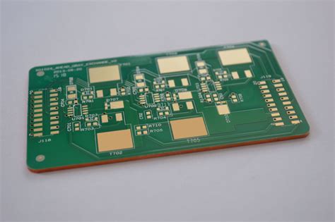
12 Layers PCB Manufacturers
Posted by
–
 Read more: 12 Layers PCB Manufacturers
What are 12 Layers PCBs? A 12 layers PCB is a printed circuit board that consists of 12 conductive layers laminated together with insulating material. These layers are interconnected through vias, which are small holes drilled through the board and plated with conductive material. The high number of layers allows […]
-
 Read more: What are the factors of PCB Aluminum thermal conductivity?
Understanding Thermal Conductivity Thermal conductivity is a material property that describes the ability of a substance to conduct heat. It is measured in watts per meter-kelvin (W/mK) and represents the rate at which heat is transferred through a material. In the context of PCBs, thermal conductivity plays a vital role […]
-
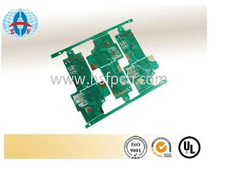
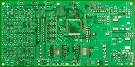
7 Working Layers in Printed Circuit Board
Posted by
–
 Read more: 7 Working Layers in Printed Circuit Board
What are the Layers in a PCB? A printed circuit board (PCB) is a fundamental component in modern electronics that mechanically supports and electrically connects electronic components using conductive tracks, pads, and other features etched from copper sheets laminated onto a non-conductive substrate. PCBs can be single-sided (one copper layer), […]
-
 Read more: About PCB Layers, You Need to Learn For Your Project
Introduction to PCB Layers Printed Circuit Boards (PCBs) are the backbone of modern electronics. They are used in almost every electronic device, from smartphones and computers to industrial equipment and medical devices. PCBs are made up of multiple layers of conductive and insulating materials, each serving a specific purpose. Understanding […]
-
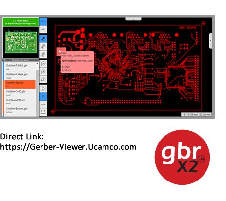
The Importance of PCB CAM Process in Prototyping
Posted by
–
 Read more: The Importance of PCB CAM Process in Prototyping
What is PCB CAM? PCB CAM, which stands for Printed Circuit Board Computer-Aided Manufacturing, is a crucial process in the production of printed circuit boards (PCBs). It involves using specialized software to convert the electronic design files, such as Gerber files, into machine-readable instructions that can be used by the […]
-
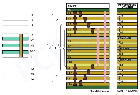
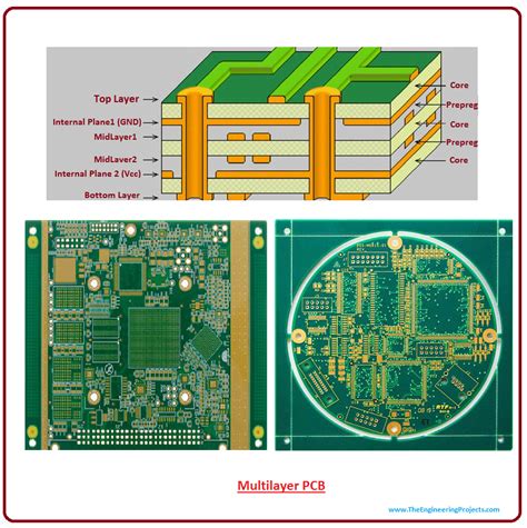 Read more: How To Determine the Number of Layers of Multilayer PCB?
Introduction to PCB Layers Printed Circuit Boards (PCBs) are the backbone of modern electronics. They provide a platform for electronic components to be mounted and interconnected, enabling the creation of complex electronic circuits. PCBs can be single-sided, double-sided, or multi-layered, depending on the complexity and density of the circuit design. […]
-
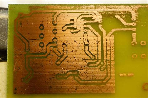 Read more: 7 Problems in the Multilayer PCB Fabrication Process
Introduction to Multilayer PCB Fabrication Multilayer Printed Circuit Boards (PCBs) are essential components in modern electronics, enabling the creation of complex and compact devices. The fabrication process of multilayer PCBs involves several intricate steps, each of which can potentially introduce problems that affect the quality, reliability, and functionality of the […]
-
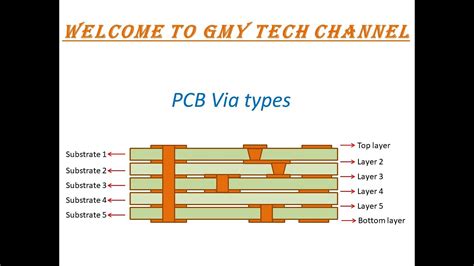
How much do you know about PCB Vias?
Posted by
–
 Read more: How much do you know about PCB Vias?
What are PCB Vias? Printed Circuit Board (PCB) vias are small holes drilled through a PCB to electrically connect different layers of the board. Vias allow signals and power to pass vertically between the layers, enabling more complex routing and denser PCB designs. Types of PCB vias There are several […]
-
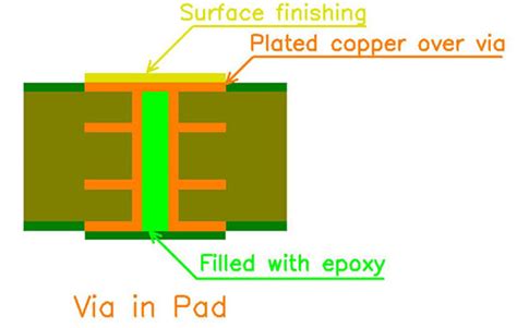
What is via in pad plating?
Posted by
–
 Read more: What is via in pad plating?
Table of Contents Introduction to Via-in-pad plating Benefits of Via-in-Pad Plating Challenges of Via-in-Pad Plating Applications of Via-in-Pad Plating Via-in-Pad Plating Manufacturing Process Design Considerations for Via-in-Pad Plating Frequently Asked Questions (FAQ) Conclusion References Request Ceramic PCB Manufacturing & Assembly Quote Now Introduction to Via-in-Pad Plating Via-in-pad plating is a […]
Recent Posts
- Best Practices to Ensure the Correct Component Orientation by Optimized assembly PCB board!

- Build a New Product quickly with PCB Assembly Prototyping – A Brief Guide!

- Can you provide complete PCB box-build services?

- Tips for Choosing the Perfect Cable Assembly Manufacturer!

- Top 10 Best PCB routing practices!

Categories
- PCB Blog 835