PCB Blog
-
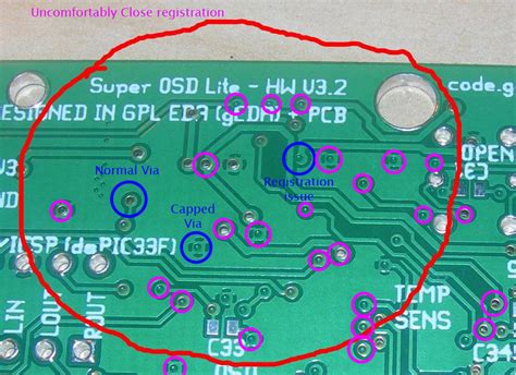
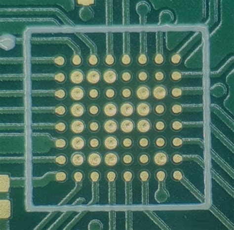
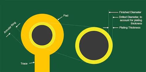
What is PCB Via?
Posted by
–
Read more: What is PCB Via?Introduction to PCB Vias A PCB via is a small hole drilled in a printed circuit board (PCB) that allows electrical connections to be made between different layers of the board. Vias are an essential component of multi-layer PCBs, enabling complex circuits to be routed in a compact space. Types […]
-
 Read more: PCB Via: What is it, and Which Type Should You Choose?
Introduction to PCB Vias A Printed Circuit Board (PCB) is a fundamental component in modern electronics, providing a platform for interconnecting electronic components. One crucial element in PCB design is the via, which allows for electrical connections between different layers of a multi-layer PCB. In this comprehensive article, we will […]
-
PCB Via Size-Complete Information It’s Here
Posted by
–
 Read more: PCB Via Size-Complete Information It’s Here
What is a PCB Via? A Printed Circuit Board (PCB) via is a small hole drilled through a PCB that allows electrical connections between different layers of the board. Vias are essential components in multi-layer PCBs as they facilitate the routing of signals and power between layers, enabling more complex […]
-
Three Ways of Treating Via in PCB Manufacturing
Posted by
–
 Read more: Three Ways of Treating Via in PCB Manufacturing
Introduction to Via Treatment in PCB Manufacturing Vias are an essential component in printed circuit board (PCB) manufacturing, allowing electrical connections between different layers of a multi-layer PCB. Via treatment is a critical process that ensures the reliability and longevity of these connections. In this article, we will explore three […]
-
Standard Printed Circuit Board Thickness
Posted by
–
 Read more: Standard Printed Circuit Board Thickness
Introduction to PCB Thickness Printed Circuit Boards (PCBs) are the backbone of modern electronics. They provide a platform for mounting and connecting electronic components, enabling the creation of complex circuits in a compact and efficient manner. One of the critical factors in PCB design and manufacturing is the thickness of […]
-
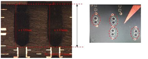
Back Drill PCB: What It Is and How to Use It
Posted by
–
 Read more: Back Drill PCB: What It Is and How to Use It
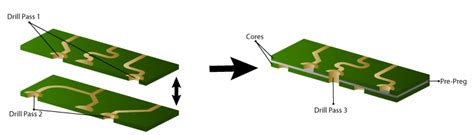
What is Back Drill in PCB? Back drill, also known as controlled depth drilling, is a PCB manufacturing process used to remove the stub left in through-holes after drilling Multilayer PCBs. By removing the unwanted portion of the plated through-hole, back drilling improves signal integrity, reduces capacitance and inductance, and […]
-
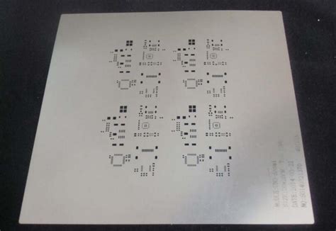 Read more: How and Why the utilization of SMT stencils simplify the Process of PCB Prototyping?
Introduction to SMT Stencils and PCB prototyping Surface Mount Technology (SMT) has revolutionized the electronics manufacturing industry by enabling the production of smaller, faster, and more efficient printed circuit boards (PCBs). One of the key components in the SMT process is the stencil, which plays a crucial role in simplifying […]
-
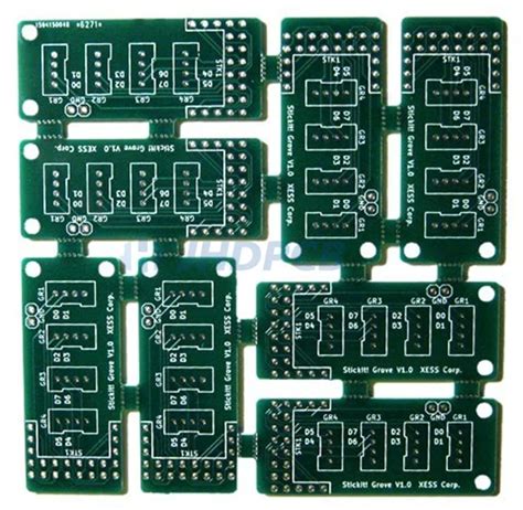 Read more: 7 Things to Know about PCB Panelization Design Guidelines for Designers
What is PCB Panelization? PCB panelization is the process of arranging multiple identical or different PCB designs on a single larger board, known as a panel. The primary purpose of panelization is to optimize the manufacturing process by maximizing the number of PCBs produced per panel, reducing material waste, and […]
-
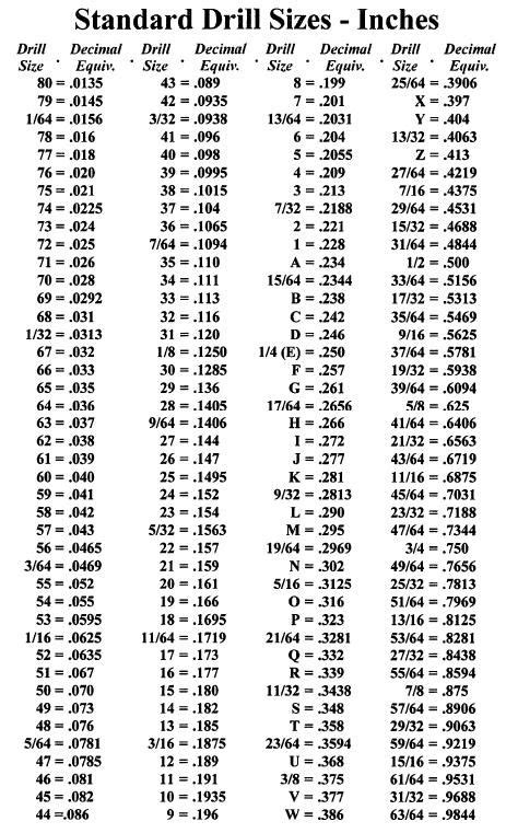 Read more: PCB Drill Sizes-A Remarkable Informative Introducing
Understanding PCB Drill Sizes What are PCB Drill Sizes? PCB drill sizes refer to the diameter of the holes drilled into a printed circuit board (PCB) to accommodate various components, such as through-hole components, vias, and mounting holes. These drill sizes are essential for ensuring proper fitment and electrical connectivity […]
-
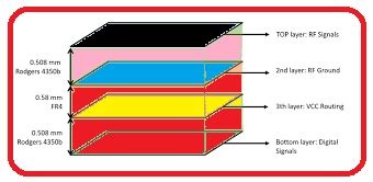
12 Layer PCB Stack Up and Thickness
Posted by
–
 Read more: 12 Layer PCB Stack Up and Thickness
Introduction to PCB Stack-up Printed Circuit Board (PCB) stack-up refers to the arrangement of copper layers and insulating materials that make up a PCB. The stack-up determines the electrical properties, mechanical strength, and overall performance of the PCB. In this article, we will focus on the 12 layer PCB stack-up […]
Recent Posts
- Best Practices to Ensure the Correct Component Orientation by Optimized assembly PCB board!

- Build a New Product quickly with PCB Assembly Prototyping – A Brief Guide!

- Can you provide complete PCB box-build services?

- Tips for Choosing the Perfect Cable Assembly Manufacturer!

- Top 10 Best PCB routing practices!

Categories
- PCB Blog 835