PCB Blog
-
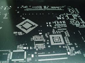
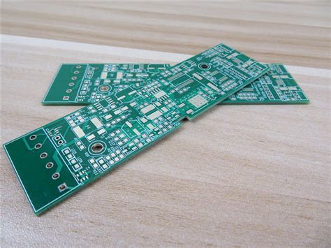
What is a PCB Stencil?
Posted by
–
Read more: What is a PCB Stencil?How PCB Stencils Work PCB stencils work by allowing solder paste to be selectively deposited onto the PCB pads through the openings in the stencil. The stencil is aligned with the PCB, and solder paste is applied using a squeegee or automated printer. The paste is forced through the openings, […]
-
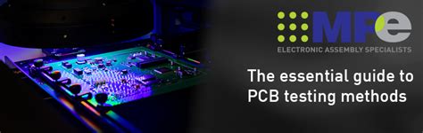
PCB ELECTRICAL TESTING
Posted by
–
 Read more: PCB ELECTRICAL TESTING
What is PCB Electrical Testing? PCB electrical testing is the process of verifying that a printed circuit board functions as intended from an electrical standpoint. It involves checking for short circuits, open circuits, incorrect component placement, and other manufacturing defects through various test methods. The goal is to ensure the […]
-
Anti-interference Methods in PCB Circuit
Posted by
–
 Read more: Anti-interference Methods in PCB Circuit
Introduction to PCB Anti-interference Printed Circuit Boards (PCBs) are the backbone of modern electronic devices. They provide a platform for mounting and interconnecting electronic components to form a complete circuit. However, as the density and complexity of PCBs increase, so do the challenges related to electromagnetic interference (EMI) and radio […]
-
 Read more: Main Factors in Printed Circuit Board Construction
PCB Materials The choice of materials used in PCB Construction plays a vital role in determining the board’s electrical, thermal, and mechanical properties. The most common materials used for PCB substrates include: FR-4 FR-4 is a glass-reinforced epoxy laminate material widely used in PCB construction. It offers excellent electrical insulation, […]
-
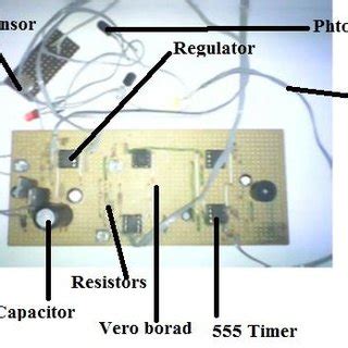
The Arrangement of Components in Assembly Design
Posted by
–
 Read more: The Arrangement of Components in Assembly Design
Introduction to Component Arrangement Component arrangement is a crucial aspect of assembly design that involves the strategic placement and organization of individual components within a larger assembly. The main goal of component arrangement is to optimize the overall performance, functionality, and manufacturability of the final product. By carefully considering factors […]
-
What is a PCB Made of?
Posted by
–
 Read more: What is a PCB Made of?
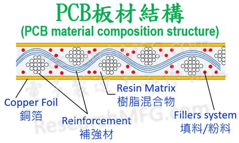
Understanding the Layers of a PCB A typical PCB consists of multiple layers, each serving a specific purpose. Let’s take a closer look at these layers and their roles in the overall composition of a PCB. Substrate Layer The substrate layer is the foundation of a PCB, providing a stable […]
-
 Read more: New PCB Architectures on High density PCB construction
What is High Density PCB Construction? High-density PCB construction refers to the process of designing and manufacturing PCBs with a higher component density and smaller feature sizes compared to traditional PCBs. This is achieved through the use of advanced materials, manufacturing techniques, and design strategies. High-density PCBs allow for more […]
-
Drilling printed circuit boards
Posted by
–
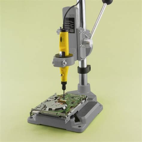 Read more: Drilling printed circuit boards
Table of Contents Introduction to PCB Drilling Types of PCB Drilling Mechanical Drilling Laser Drilling Drilling Machines and Tools CNC Drilling Machines Drill Bits Depth Control Systems Drilling Parameters and Considerations Drill Bit Selection Spindle Speed and Feed Rate Hole Accuracy and Tolerance Drill Breakout and Deburring Challenges in PCB […]
-
 Read more: Prepreg vs. Core: What Are Their Role in PCB Manufacturing
Introduction to Prepreg and Core in PCB Manufacturing Printed Circuit Boards (PCBs) are essential components in modern electronics, forming the backbone of various devices and systems. The manufacturing process of PCBs involves several key materials, among which prepreg and core play crucial roles. In this article, we will delve into […]
-
Isola Introduces Low-Loss I-Tera? MT40 Circuit Material Supporting Multilayer PCBs for LEO Satellites
Posted by
–
 Read more: Isola Introduces Low-Loss I-Tera? MT40 Circuit Material Supporting Multilayer PCBs for LEO Satellites
New High-Performance Laminate and Prepreg System Enables High-Reliability Satellite PCB Designs Isola Group, a market leader in copper-clad laminates and dielectric prepreg materials, has launched I-Tera MT40, a new low-loss, high-performance circuit material designed to support multilayer printed circuit boards (PCBs) for low Earth orbit (LEO) satellites. The innovative laminate […]
Recent Posts
- Best Practices to Ensure the Correct Component Orientation by Optimized assembly PCB board!

- Build a New Product quickly with PCB Assembly Prototyping – A Brief Guide!

- Can you provide complete PCB box-build services?

- Tips for Choosing the Perfect Cable Assembly Manufacturer!

- Top 10 Best PCB routing practices!

Categories
- PCB Blog 835