PCB Blog
-
Read more: What is the Basic Stack up of 16 Layer PCB Board?
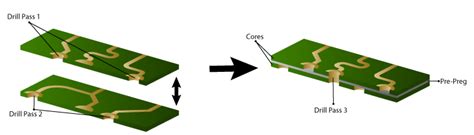
Introduction to PCB Stack-up Printed Circuit Board (PCB) stack-up refers to the arrangement of copper layers and insulating materials that make up a PCB. It is a critical aspect of PCB design, as it determines the board’s electrical properties, signal integrity, and manufacturability. In this article, we will focus on […]
-
What Is A 6 Layer PCB Board?
Posted by
–
 Read more: What Is A 6 Layer PCB Board?
Key Characteristics of 6 Layer PCB Boards Increased Routing Density One of the main advantages of using a 6 layer PCB is the ability to route more traces on the board. With six layers to work with, PCB designers have more flexibility in placing components and routing connections between them. […]
-
 Read more: Multilayer Pool – What You Need To Know About Multilayer PCB
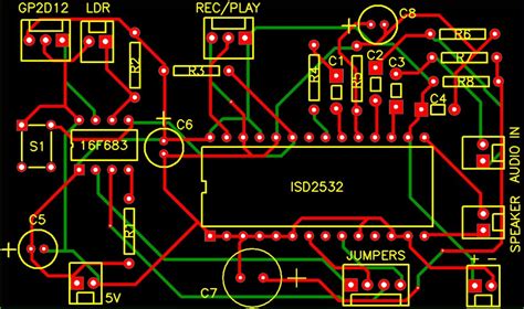
Introduction to Multilayer PCB A Multilayer PCB, also known as a multilayer printed circuit board, is a complex printed circuit board that consists of multiple layers of conductive copper foil laminated together with insulating material. These layers are interconnected through plated holes called vias, which allow signals to pass from […]
-
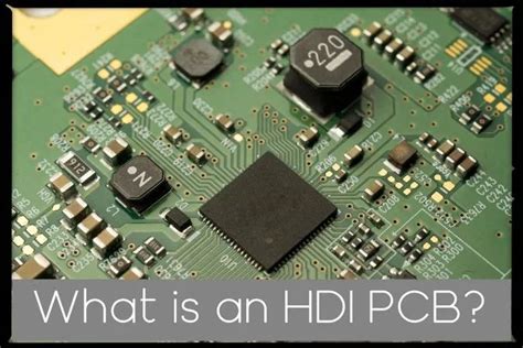 Read more: HDI PCB-The Ultimate Guide To How To Achieve A Perfect HDI
What is HDI PCB? HDI PCB, or High Density Interconnect Printed Circuit Board, is a type of PCB that features a higher wiring density per unit area than conventional PCBs. This is achieved through the use of smaller vias, finer trace widths and spaces, and more precise layer-to-layer registration. HDI […]
-
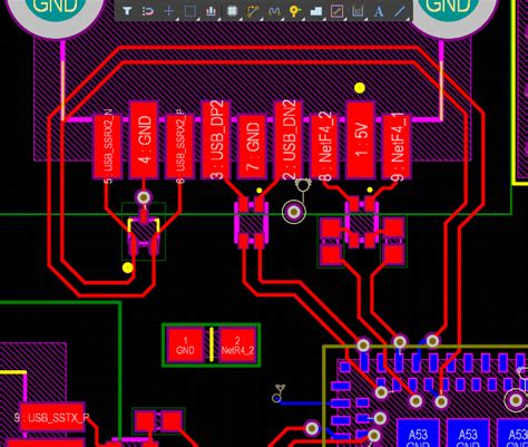
Guide to Create A PCB with KiCad
Posted by
–
 Read more: Guide to Create A PCB with KiCad
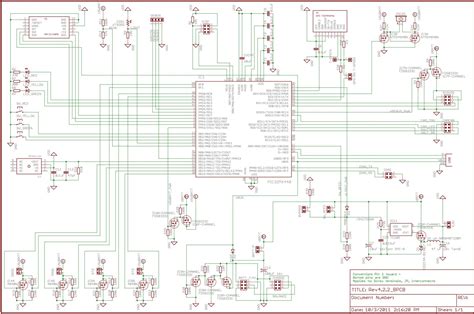
Introduction to KiCad and PCB Design KiCad is a free and open-source electronic design automation (EDA) software that enables users to design printed circuit boards (PCBs). It provides a complete set of tools for schematic capture, PCB layout, and gerber file generation. In this comprehensive guide, we will walk you […]
-
High Frequency PCB Layout
Posted by
–
 Read more: High Frequency PCB Layout
Introduction to High Frequency PCB Layout In today’s world of electronic devices, the demand for high-speed and high-frequency applications is constantly growing. From smartphones to aerospace systems, the need for efficient and reliable printed circuit boards (PCBs) that can handle high-frequency signals is paramount. However, designing a PCB layout for […]
-
 Read more: What s The Difference Between Pre Layout And Post Layout PCB Simulation
Introduction to PCB Simulation PCB (Printed Circuit Board) simulation is a crucial step in the design and development of electronic devices. It allows engineers to test and validate the performance of their PCB Designs before the actual manufacturing process begins. PCB simulation can be divided into two main categories: pre-layout […]
-
5 tips for PCB schematic file management
Posted by
–
 Read more: 5 tips for PCB schematic file management
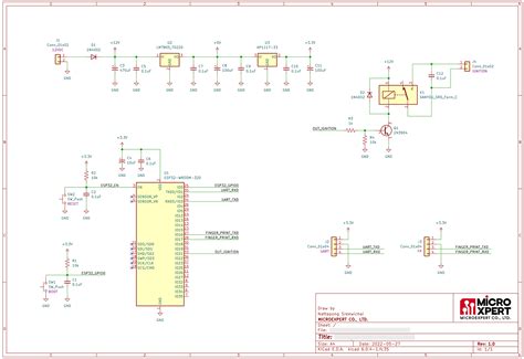
Introduction Printed Circuit Board (PCB) design is a complex process that involves creating a schematic diagram, which is a graphical representation of the electronic components and their interconnections. Managing PCB schematic files is crucial for ensuring the accuracy, consistency, and efficiency of the design process. In this article, we will […]
-
Why PCB design uses 3D functions
Posted by
–
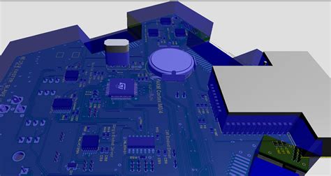 Read more: Why PCB design uses 3D functions
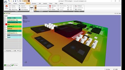
Introduction to PCB 3D Design Printed Circuit Board (PCB) design has evolved significantly over the years, with the introduction of 3D functions playing a crucial role in enhancing the design process. PCB 3D design allows engineers and designers to visualize and optimize their designs in a three-dimensional space, leading to […]
-
 Read more: PCB Layout in right angle alignment the differential traces and serpentine lines
Introduction to PCB Layout and Differential Traces Printed Circuit Board (PCB) layout is a crucial aspect of electronic design, as it determines the performance, reliability, and manufacturability of the final product. One of the key challenges in PCB layout is ensuring the proper alignment and routing of differential traces and […]
Recent Posts
- Best Practices to Ensure the Correct Component Orientation by Optimized assembly PCB board!

- Build a New Product quickly with PCB Assembly Prototyping – A Brief Guide!

- Can you provide complete PCB box-build services?

- Tips for Choosing the Perfect Cable Assembly Manufacturer!

- Top 10 Best PCB routing practices!

Categories
- PCB Blog 835