PCB Blog
-
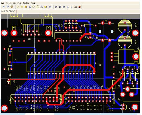
The way of using Altium pcbDoc with Eagle
Posted by
–
Read more: The way of using Altium pcbDoc with EagleIntroduction to Altium pcbDoc and Eagle Altium pcbDoc and Eagle are two popular PCB design software tools used by engineers and designers worldwide. While both have their strengths and weaknesses, integrating them can provide a powerful solution for PCB design projects. In this article, we will explore the process of […]
-
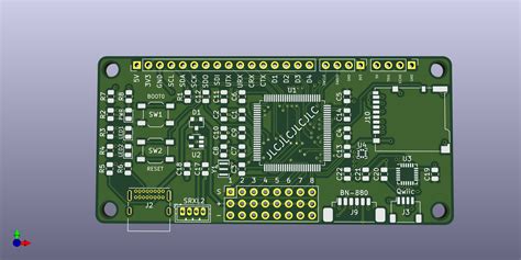
The way to produce Castellated-Hole-PCB
Posted by
–
 Read more: The way to produce Castellated-Hole-PCB
Introduction to Castellated-Hole-PCB Castellated-Hole-PCB, also known as castellated printed circuit boards or castellated hole technology, is a specialized PCB design that features a series of semi-circular holes or slots along the edges of the board. These holes, resembling the battlements of a castle, serve as electrical contacts and mounting points […]
-
Tips and Essentials for PCB Wiring
Posted by
–
 Read more: Tips and Essentials for PCB Wiring
Introduction to PCB Wiring Printed Circuit Board (PCB) wiring is a crucial aspect of electronic design and manufacturing. Proper PCB wiring ensures the reliable operation of electronic devices, minimizes signal interference, and enhances the overall performance of the system. In this comprehensive guide, we will explore the essential tips and […]
-
To Bond Circuit Board Jumper Wires
Posted by
–
 Read more: To Bond Circuit Board Jumper Wires
Introduction to Jumper Wires and Circuit Bonding Jumper wires are a crucial component in electronic circuits, allowing you to create temporary or permanent connections between different points on a circuit board. These small wires come in various lengths, colors, and connector types, making them versatile for a wide range of […]
-
RS-274X (Extended Gerber)
Posted by
–
 Read more: RS-274X (Extended Gerber)
What is Gerber? Gerber is a vector image file format that describes the layout of a PCB. It contains information about the copper traces, solder masks, silkscreen layers, and drill holes that make up the board. Gerber files are used by PCB Manufacturers to create the physical boards from the […]
-
To make sense of so many PCB design software
Posted by
–
 Read more: To make sense of so many PCB design software
Key Considerations When Choosing PCB Design Software Before we get into comparing specific PCB design software, it’s important to understand the key factors you should consider when evaluating your options: Ease of Use PCB design can be complex, so having software with an intuitive interface and easy learning curve is […]
-
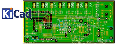
To make a PCB with KiCad
Posted by
–
 Read more: To make a PCB with KiCad
Introduction to PCB Design and KiCad Printed Circuit Boards (PCBs) are the backbone of modern electronics. They provide a platform for electronic components to be mounted and interconnected, enabling the creation of complex circuits and devices. Designing a PCB can be a daunting task, especially for beginners. However, with the […]
-
 Read more: First attempt at USB differential pair routing on a 2 layer board Acceptable
Introduction to USB routing USB (Universal Serial Bus) has become the standard interface for connecting various peripherals to computers and other electronic devices. Proper USB routing is crucial for ensuring reliable data transmission and minimizing signal integrity issues. When designing a 2-layer printed circuit board (PCB), routing USB differential pairs […]
-
What is Soldermask (SM)?
Posted by
–
 Read more: What is Soldermask (SM)?
Introduction to Soldermask (SM) Soldermask, often abbreviated as SM, is a vital component in the production of printed circuit boards (PCBs). It is a thin, protective layer applied to the copper traces of a PCB to prevent solder from adhering to areas where it is not intended. Soldermask also serves […]
-
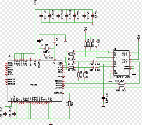
Creating the Layout from your Schematic
Posted by
–
 Read more: Creating the Layout from your Schematic
Introduction to Layout-Schematic Relationship The process of creating a printed circuit board (PCB) involves several crucial steps, and one of the most important is translating the schematic design into a physical layout. The schematic represents the logical connections between components, while the layout determines their physical placement and routing on […]
Recent Posts
- Best Practices to Ensure the Correct Component Orientation by Optimized assembly PCB board!

- Build a New Product quickly with PCB Assembly Prototyping – A Brief Guide!

- Can you provide complete PCB box-build services?

- Tips for Choosing the Perfect Cable Assembly Manufacturer!

- Top 10 Best PCB routing practices!

Categories
- PCB Blog 835