
PCB Blog
-
Read more: Land Pattern-How Do We Design it to Meet Industry Standards
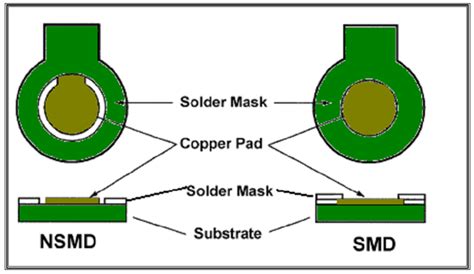
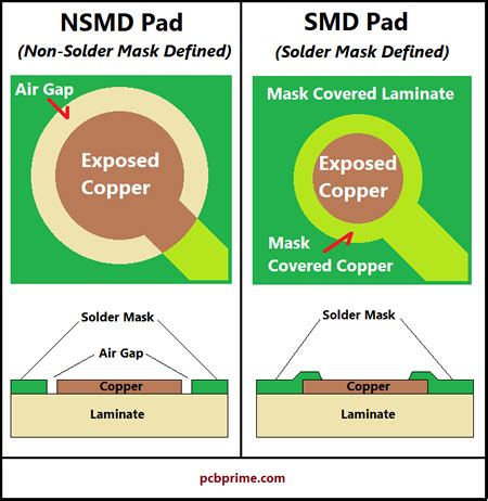
What is a Land Pattern? A land pattern, also known as a footprint or pad layout, refers to the arrangement of copper pads on a printed circuit board (PCB) where electronic components are soldered. The design of land patterns plays a crucial role in ensuring the reliability and manufacturability of […]
-
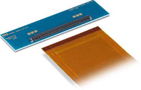
FFC vs FPC: The Main Differences Between the Two
Posted by
–
 Read more: FFC vs FPC: The Main Differences Between the Two
Introduction When it comes to flat flexible cables, two common types are often compared: FFC (Flat Flexible Cable) and FPC (Flexible Printed Circuit). While they may look similar at first glance, there are some key differences between FFC and FPC in terms of their construction, applications, and properties. In this […]
-
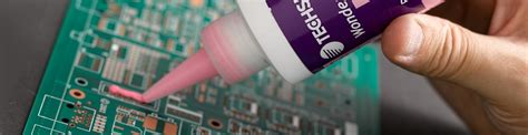
How Can You Repair the Solder Mask on a PCB?
Posted by
–
 Read more: How Can You Repair the Solder Mask on a PCB?
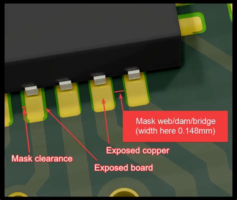
What is Solder Mask and Why is it Important? Solder mask, also known as solder resist or solder stop mask, is a thin layer of polymer applied to the copper traces of a printed circuit board (PCB). Its primary purpose is to protect the copper traces from oxidation, prevent solder […]
-
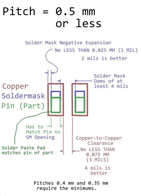 Read more: Soldermask Expansion is the value applied to SMD pads
What is Soldermask Expansion? Soldermask expansion, also known as solder resist expansion or solder mask pullback, refers to the distance or clearance between the edges of surface mount device (SMD) pads and the soldermask opening on a printed circuit board (PCB). It is a critical design parameter that ensures proper […]
-
 Read more: Why is Green Soldermask Most Commonly Used for PCB Fabrication?
Introduction to PCB Soldermask PCB (Printed Circuit Board) soldermask is a protective layer applied to the copper traces of a PCB during the manufacturing process. Its primary purpose is to prevent solder bridges from forming between adjacent pads or traces, which can cause short circuits and other issues. Soldermask also […]
-
 Read more: How to Remove Soldermask from Printed Circuit Boards?
What is PCB Soldermask? PCB soldermask, also known as solder resist or solder stop mask, is a thin layer of polymer applied to the copper traces of a printed circuit board. Its primary functions are: Preventing solder bridges from forming between adjacent traces during assembly Protecting the copper from oxidation […]
-
What s the impact of the soldermask thickness?
Posted by
–
 Read more: What s the impact of the soldermask thickness?
Introduction to Soldermask Thickness Soldermask, also known as solder resist or solder mask, is a thin layer of polymer applied to the copper traces of a printed circuit board (PCB) to protect them from oxidation, prevent solder bridges, and provide electrical insulation. The thickness of the soldermask plays a crucial […]
-
QFN Packaging: Types, Assembly, and Benefits
Posted by
–
 Read more: QFN Packaging: Types, Assembly, and Benefits
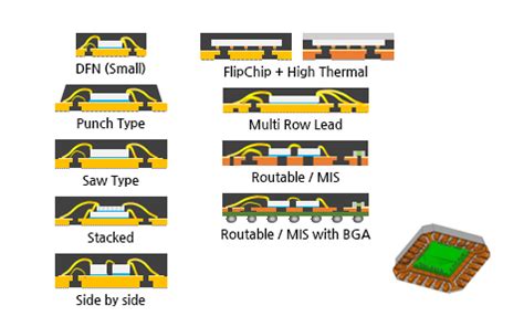
Introduction to QFN Packaging QFN (Quad Flat No-lead) packaging is a surface-mount technology that has gained significant popularity in the electronics industry due to its numerous advantages over traditional packaging methods. This advanced packaging technique offers reduced package size, improved thermal and electrical performance, and cost-effectiveness, making it an ideal […]
-
 Read more: The common problems and solutions of PCB soldermask
What is PCB Soldermask and Why is it Important? PCB soldermask, also known as solder resist or solder mask, is a thin layer of polymer that is applied to the copper traces of a printed circuit board (PCB). The main purpose of soldermask is to protect the copper traces from […]
-
4 Main Types of PCB Solder Mask
Posted by
–
 Read more: 4 Main Types of PCB Solder Mask
Introduction to PCB Solder Mask Printed Circuit Boards (PCBs) are essential components in modern electronics, providing a platform for electrical components to be mounted and connected. One crucial aspect of PCB manufacturing is the application of a solder mask, which serves several important functions. A PCB solder mask is a […]
Recent Posts
- Best Practices to Ensure the Correct Component Orientation by Optimized assembly PCB board!

- Build a New Product quickly with PCB Assembly Prototyping – A Brief Guide!

- Can you provide complete PCB box-build services?

- Tips for Choosing the Perfect Cable Assembly Manufacturer!

- Top 10 Best PCB routing practices!

Categories
- PCB Blog 835