PCB Blog
-
PCB Milling – How To Make(Helpful)
Posted by
–
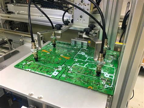
Read more: PCB Milling – How To Make(Helpful)What is PCB Milling? PCB milling is a subtractive manufacturing process that uses a rotating cutting tool to remove copper from a substrate, creating the desired circuit pattern. The milling machine is controlled by a computer, which interprets the PCB design files and guides the cutting tool along the appropriate […]
-
 Read more: China PCB Industry Ranking & Domestic PCB Enterprise Ranking
Introduction to the PCB Industry in China The Printed Circuit Board (PCB) industry is a crucial component of the electronics manufacturing sector, and China has emerged as a global leader in PCB production. With a vast domestic market and a strong export presence, the Chinese PCB industry has experienced significant […]
-
Class Carrier Mobile Phone PCB
Posted by
–
 Read more: Class Carrier Mobile Phone PCB
Introduction to PCB-Phone Technology In the rapidly evolving world of mobile technology, the printed circuit board (PCB) plays a crucial role in the functionality and performance of smartphones. The PCB-Phone, a class carrier mobile phone PCB, represents a significant advancement in the field, offering enhanced features and capabilities that cater […]
-
Cleaning of ICT Probes
Posted by
–
 Read more: Cleaning of ICT Probes
Introduction to ICT Probe Cleaning ICT (Information and Communication Technology) probes are essential tools used in various industries, including telecommunications, networking, and data transmission. These probes are designed to monitor, analyze, and troubleshoot network performance, ensuring optimal functionality and reliability. However, to maintain the accuracy and longevity of ICT probes, […]
-
Comprehensive Guide to X-ray Inspection
Posted by
–
 Read more: Comprehensive Guide to X-ray Inspection
What is X-ray Inspection? X-ray inspection is a process that utilizes X-rays to create images of an object’s interior. X-rays are a form of electromagnetic radiation with wavelengths shorter than visible light. When X-rays pass through an object, they are absorbed or scattered depending on the object’s density and composition. […]
-
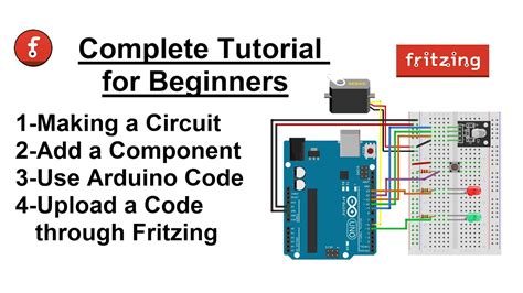
Creating A PCB In Everything with Fritzing
Posted by
–
 Read more: Creating A PCB In Everything with Fritzing
What is Fritzing and Why Use It for PCB Design? Fritzing is an open-source software tool that allows users to easily design and create printed circuit boards (PCBs). It provides a user-friendly interface for designing electronic circuits, from simple breadboard layouts to complex PCBs ready for production. Some key features […]
-
 Read more: Power PCB Design: Five Major Things That Beginners Need to Know
Understanding the Basics of Power PCB Design Before diving into the specifics of power PCB design, it’s essential to understand the basics. A power PCB is a printed circuit board that is designed to distribute power to various components within an electronic device. The main goal of a power PCB […]
-
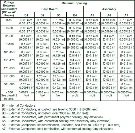
Detailed PCB safe distance
Posted by
–
 Read more: Detailed PCB safe distance
Understanding PCB Safe Distance and Its Importance When designing and manufacturing printed circuit boards (PCBs), one critical factor to consider is the PCB safe distance. This term refers to the minimum spacing required between various elements on a PCB, such as traces, pads, and components, to ensure proper functionality, reliability, […]
-
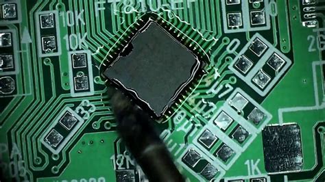
Board layout of QFN for more reliable soldering
Posted by
–
 Read more: Board layout of QFN for more reliable soldering
Introduction to QFN Packages and Soldering Challenges Quad Flat No-lead (QFN) packages have become increasingly popular for integrated circuits due to their small size, low profile, and good thermal and electrical performance. However, the small pitch and hidden leads underneath the package make QFNs more challenging to solder reliably compared […]
-
 Read more: Hole edge to solder mask edge clearance used in tented vias
What is Solder mask clearance? Solder mask clearance refers to the minimum distance between the edge of a drilled hole (such as a via or through-hole) and the edge of the solder mask opening around that hole on a printed circuit board (PCB). This clearance is an important design parameter […]
Recent Posts
- Best Practices to Ensure the Correct Component Orientation by Optimized assembly PCB board!

- Build a New Product quickly with PCB Assembly Prototyping – A Brief Guide!

- Can you provide complete PCB box-build services?

- Tips for Choosing the Perfect Cable Assembly Manufacturer!

- Top 10 Best PCB routing practices!

Categories
- PCB Blog 835