What is Differential Trace Impedance?
Differential trace impedance refers to the Characteristic Impedance of a differential pair of traces on a printed circuit board (PCB). A differential pair consists of two conductors that carry equal and opposite signals. The impedance of the pair is determined by the geometry and spacing of the traces as well as the properties of the dielectric material surrounding them.
Differential signaling is commonly used for high-speed digital interfaces like USB, PCIe, HDMI, Ethernet, and more. It offers advantages over single-ended signaling such as:
- Improved noise immunity
- Reduced electromagnetic interference (EMI)
- Ability to drive signals over longer distances
To achieve these benefits, it’s important to carefully control the differential impedance of the traces. Mismatched impedance can lead to signal reflections, increased EMI, and degraded signal integrity.
Calculating Differential Impedance
The differential impedance of a pair of traces depends on several factors:
- Trace width (w)
- Trace thickness (t)
- Spacing between traces (s)
- Height above reference plane (h)
- Dielectric constant of material (εr)
There are various formulas and online calculators available to determine the differential impedance based on these parameters. One common approximation is:
Zdiff ≈ 2 × 87 / √εr × ln(1.9 × (2h + s) / (0.8w + t))
Where:
– Zdiff = differential impedance in ohms
– εr = dielectric constant of material
– h = height above reference plane in mils
– s = spacing between traces in mils
– w = trace width in mils
– t = trace thickness in mils
For example, consider a differential pair with the following properties:
| Parameter | Value |
|---|---|
| Trace width (w) | 5 mils |
| Trace thickness (t) | 1.4 mils |
| Spacing between traces (s) | 5 mils |
| Height above reference plane (h) | 5 mils |
| Dielectric constant (εr) | 4.5 |
Plugging these values into the equation above yields:
Zdiff ≈ 2 × 87 / √4.5 × ln(1.9 × (2×5 + 5) / (0.8×5 + 1.4))
≈ 2 × 87 / 2.12 × ln(15 / 5.4)
≈ 82 × 1.022
≈ 84 ohms
So this particular geometry would have a differential impedance of approximately 84 ohms. Common target impedances are 90 ohms for USB and 100 ohms for Ethernet and PCIe.

Designing for Target Impedance
To hit a specific target impedance, PCB designers can adjust the trace geometry and spacing. Typically the dielectric material and thickness are constrained by other factors, so the main variables are:
- Trace width
- Spacing between traces
In general, increasing the trace width will decrease the impedance, while increasing the spacing will increase it. Online calculators and field solver tools help designers converge on the right values.
Many PCB design tools have built-in features to calculate and tune differential impedance. The software models the trace cross-section and computes the impedance based on the Layer Stack-Up and material properties. More advanced field solvers use numerical methods like finite element analysis for greater accuracy.

Impact of the Reference Plane
The discussion so far has assumed the presence of an uninterrupted reference plane beneath the differential pair. This is typically a ground plane or power plane on an adjacent layer.
The reference plane serves several important functions:
– Provides a controlled return path for the differential currents
– Minimizes loop area and reduces inductance
– Shields the traces from external noise coupling
– Confines the electromagnetic fields to enable consistent impedance
However, in some cases it may not be possible or practical to provide a solid reference plane. Reasons could include:
- Limited board space or layer count
- Cut-outs or apertures required for components, mounting holes, etc.
- Traces crossing splits in reference plane (e.g. different voltage areas)
Without a continuous reference plane, the impedance of the differential pair becomes more difficult to predict and control. The fields are no longer confined between the traces and the plane. Energy can couple into other structures or radiate as EMI.
 QTPAuthZwrCZ4iYmbaqM+xioZyoZvL3PXaDUY9Rms38T+IGAtLKeNYbDRZWVp7mS2JleGxYgE7cbo0GFdgzCN/sz0hun8vHiPxWPM8rbv0mwTHmeRjdv0kY/1q5zjGHzjyX8oAt+GP8AkWvCn/YD0n/0kjrXrL06XT7Kx0uwt11Iw2tpZWcDT2F8JDGkdtEhlJgUA4kTdwMYfOPJbyr9vcRXKF41nUDy+Li3uLdvniSYYW4RW6MAeODlThkIUAyvFcsMPhjxU8skcaHRtRiDSMqqZJYHiRAW7sSFUdyQO9cprhQ6V4j05pYDoWnaVqmr2EgmiMU0V/aqulw53eUYhK90tuqqNv2WDGMKbj0KWRYYpZXEhSKN5GEUckshVQWISOIFyfQAEnsKyItekee9tZNE1mG4tLS2ujG406VpBdTPbwRp9lupOWKPy21VCksyjkgHPp4kWbUdUt08UWMWnQX13LBqEj6a9up+y6dNbWMsgCxmJme64DLIwgIEgMTGs7TtavbbTLBLXWv3cHg3w/e6XZi3tZUu9WSK6tTpqTiPJ8xocNFu8xmzsZBEy16HZXkN/bpcxLIgMk8MkcoUSRT28r280T7SVyjKykhiDjIJBBMMWnCLVL3Vftl2z3dpbWbWzi2+zRx2zO8ZTbEJsgvIeZD/AKw+gEYBx02v6kmk6hdLrmLtfDl5qeoLt07/AIkWsxG2MGnbDDlfMZ5Y9ku9z5eAQyktYt9fkn1S7hh8SWk+n3HiD+xrZoTpzSW0d7o7X0UkcyKUYiVDFBuQ5+cN5jY8jt6ZI7IoZYpJSZIkKxmMMFd1QufMZRhQSzc5wDgE4DAHHabem38I+BjHqvkWk8FlbahqmbL/AECJLKaTb5ksZtl2yJHb/Oh+9tPzndTLW4j1HXfDsd/qMc32jRvFlqtpKLEx6nYrqEMEE7xmLcwuI080lcK3lZUBNyv29FABUV1c29lbXd5cv5dtaQTXNw+1m2RRIZHbagLHABPANS0UAeeySaVcyaf5Yjz/AGzaraNfR2rMr+I7yW51fQ71Jw8KzIiyFgCrgOkfJY/bC+1rVZofEF1JrMmn2cd3rfhuJWn0qG2GpyXR0+yeKRA16oiXM9wWkVhgMgKDbXdWN5DqFpbXsCyC3uoxNbmQKGkgY5jlABOA4wyg4IDDIU5Vc3SfDtlpMtvMtzd3c1rpsekWcl4tmJLexQqwgDWkERYZVT8+4jHBG9t4BU0B4bq+mkS602+h0zTbay0+60SJYNMhjuZGM1nHEksw8xRDAz/vjhSgCJktcP0208ZRXtu+o3vmWa+Z5yf2hZTbsxsF/dxaJbsecdJ1/HG1uiqpf36afHayyQTyxz31jYEweV+5a8mW2jkkEjqdu5lB27j83TAJABDczeJEnkWz07SprYbfLkudUubeVvlBO6KOwlUYOQP3h9eM4HF6lqWj3ttq+oWU2PMz4isri6SFH0zWoUttI09547pWiWK6Uo8JlRcKGkyMhrT0WigDi59UmttV1OIX/wDZeheF57Jb5IV0tbP+zjp0c8UIiZJLwSvI4RdqqpRCqnzB80Oj3NxJ4p0y71Q6VFfazoeqXdrHaamt5J9lkk05re2QeUo2qscjjbI6sxmcbQcDoLbw7ZW99DfNc3dwba71S9sYbhbPy7OfUpJJLgwyQwJPg73G1pWHI4JQFNWG5t55L2KJ90llOttcjaw8uVoYrkLlgAfldDxnr6jAAJaKKKACimF2EscYikKNHI7Sgx+WjKUARgW35bJIwpHynJHAd9ABRRVHT9RGowxTJZ3cKNJqEMouDbboJ7K6Nm8UnkyvkkhipXcMKckZAYAvUUVXivIZbu9stsi3FpHbTMHC7ZILkOI5UKk8EpIuDg5jPGCGkALFFFFABRRRQAUUUUAFFFFABRRRQAUUUUAFFFFABRRRQAUUUUAFFFFABRRRQBnXetabZXJs5RfSXKwRXLpZabqN7sileSNGdrOF1GSjgZI+6ah/4SHS/wDn31z/AMJ/Xv8A5EpiGYeIPERhSN5h4f0AxJK7RxvILnV9qvIqsQCep2HHoehhs7jxVPPqsa3OjXNvbxxW9vcx2F3bRG+MzJcKd13LuEAA3AYDMxTehiYqACa/Yi+u3Nt4g8lrSzWMnQPEHlmRZLguFHlEZwVz+5XqPmfG23s/8JDpf/Pvrn/hP69/8iVUi1jWLyPRYLNLEXl7/as0k9ws32OSwsJhZ/bbZY2LHzDJBNEu8hkJHmDIkOjpd3eXB1W2vDA9zpl8tlJNbRvDFPvtLe9DrDJJIy4EoUjzGztzkbtqAFmK8hubGK/s1kuYZ7RLy1WIKklxHJGJYwguCgBYEY3FevOO2Va6/d3ttaXlt4b1yS2u4Ibm3fzdDXfFKgkRtr6gGGQQeQKm8Mf8i14U/wCwHpP/AKSR1RubG+82+0KOCRtJ1e7N5LcADy7ezuTJNqVox+9mR+Ad4b/TSUGLM4ANGLVZ7vRItXsNMu55bq0S6srGWW0gnmWXBi3yGVoVBBDH5yQD0LDZWRBL4mtrFoIND1IXMslob/UHm0U311PLHKLm8jt2u3gyNkSxhpsKJAAjJb+XJ01zc29nBJcXD7Io9oJCs7MzsERI0QFmZiQqqASSQACTg5qa9ZTanpWnwJPINQsdQvFnEF0Eia0lihaGXMW1WBLhwzKUZArANKAQCpqenS3PhC/0+LSM3d3pTqunma3naK/uF3lpLm5dUZkkO9pC+SVLcsfmzYNAmh1W4vW06+ktJIJJFtHm0t0e0l04RS6ddPNvuJJXmMkjqbgRFn8wuXyJN0eI9Ea2iu1a+MUt9NpsSjS9UNxJdwpI8kaW4g847Qj7jswChGcqQKNx4v0e1064nE0l7e2+jQ6sIbex1CFbqGW2adLiNWjkKwsRhnJYISFZg3DAGFYaJrlja6WY9J1Jbiy03wtJsXULVv8ATrPUDFqO0PebPMkg2pGxOPKHlbkH7osj0fxBbNNG+h311/p3hnUldJdE+zpqFhfvPfXFqZLhJz5iYVJJcysOJG4465PEmguVDXE8GZ7m2Y3tlfWixS29oNQkWdrqJAn7s7xuIyAcZ2nDH1gy3Xh77E8Ztb3UrrTb+G6tbmG8hkXT7i+j+SYo6H92CQ0R3LICMDBcA5RdE1eC28q20HVYILufXIr22s73Ro2W1m1i1vrRRHPPJamJYvPTytpXLyKQBcGR+x0CzmsNJtLaa2tLWQSXczW9kjRwRC4uZbgKsZllCnDDcqysoOQpKgGtSigAqjrNnNqGka3YQtGs19pt9ZxNKWEayTwPEpcqCcZPPBq9TJRMYpRC8aTGNxE8qNJGkhB2s8aspIB6jeM+o6gA5poE1m/0zVG0v7ZaSwaS9n9qkiik0O9srya4ujMNxkSX/VoyoG3NBsfao3VkTaBqT6TqFquh5u28OXmmag27Tv8Aie6zKbYQajvM2W8tklk3y7HHmZALMQu7p/iayXT9Ak1m7ggv9U0qHVgIrW6htTFIEdxG7mRf3QYGX95woMhCpyluTxJ4djS1kN7ujup5bW3eKC5lWS4SLz1iUxRkbpFIaAdZAwKbw43AGFDpF6l+r/2RfGxfVYFkiuby1uE/se90VobqGSOW6cH/AEg+ZdcEyNh8ylQVyNM03VjpHhS5sdEnIWx8Py37W93Zs2p+VeabqUM5e6mjc+VHDLGFfGwzBE3R5dO0Ot+GrxJ7eW6geCSC4W6F3FIlqoSJnmtbl50ESyqoZpImIcKCSoAJGdp2uaTa3OqWMCQQaZZwaW9jZ2Wl3lvfRXF6940tu9gqmYtiLzgBbqdrliCo3kAxU8OarBpLwT6fqV9dnUvDs85W60qKRrqxufOvNRs3hMDAyLlVlebzm3AMFCbmfPoWvbZLe2sb6KGafWra6MV1Ysj6dHq1peWUMMNxM0XleQs0EMZj2q0jBkVJmdurXxBoDXaWK30f2iSOzmiGyURTQ3gPkTRTFfKaNjhAwYjcypndIFZi+JNBfz9lxO5i+zlVjsr53uVuPOMT2SLEWlVhHIwaMONqFs7RmgDl7vw9qRjsVt9Lvmubfw54it7a7e705JILyeZbrTYJTbvCv7kqfLVYikTMmwny/NSHVdA1eeXxFc2Ohz28t5O+oWclq2jJdfbpdOtFhZzNM0S+VKtwZHXEitKDE5Erk91PqWnW9tb3bTeZBc+X9lNokl29z5iGRfs8VqryP8oLfKp+UFuikitF4g0CYRMl9GIpbRLxZpUlitxE1uLwK88qiMSeX+9KFgwT5iu3mgDmZNAtb2LxleX+hwWEkl9DrGnPrTae9nG0NtbSSGZbaaZEWSSJjdEBS6OMsSP3VxdIL6Dq1xFps66h4gvk1G+islsrO/ktZr4Sxw3C3qfZ9yQnbNGw2sfMBJMxd9G71rwrImnPfDfm+IskvNNuzLDqNvF56J5UsPmJOVOYVKqzbhsDbhl+p6yti/hu5S4tG0vUruS2mdY5J5JlksZ7u3azeB+SxQKqiNy/mALz98A53+zbvS4YriTS49Pih8MeK4r6+0p4bOKyF3dDUIUG2W4uVKBXJEaTKjSfJuX7sI0e3+wX1nD4ekXWX1nw/q95bWMGl6a9vaxTqiT2Tw3zqgKQzouLsvvdzhFlyOu/t/RzLbQo93JLcWl1eRLDp+oSkxWpKTq3lwnEiEbHQ4YMQpXc4DQ2k2kWug3OpeHtMjNq9pc6la2llZvYteyLESu2Hyg+ZNqhT5ZyMEZGMgHNTaT4jjnspotMvmGl6qw00Wc+k/Lp66zLcuim7nBjia3aOKNYjGTsZJB5aIKrXmka1dQaijeFbtprrTfGVmHll0Ikyapqq6lYl2N4TiI7mPXaxyuc5rprLWr9b2a21GbSmtBYpqVtfwfaLe3utPSMyT30bMZrcKpeCPabjON0hIV1Vra+IdJkttWuYhfN/ZmxLiGSwvLW4e4lQPFbQpexx7pXygRQckyL/wA9BuAOR1DS7q4uJ9Jk0m+ezu/tV3aWk0lheSLaTWWmw3U0C3V2sS3UUpkJlaZiGuGYJN57vB0drPZ3eoWF7pEPm6fpfhyZIo7VEhWT+0jZ3VtbW6yFEVgkILKxTaJoz0fKWLFYfEGmA63p2mzvFqWqwtbvGt1bRyWV7c2SshuU5OF+9sXOTwudo2qACiiigAooooAKKKqaje/YLVrgRebI09naQRltitcXlxHaRCR8EhdzruIViBkgMRtYAt0Vi6droum1VL22jsX0uSdb0yXls6QRwpGfOmDFJVjkPmmEtENyRbzt8wKWTa/9on06Dw//AGVqxuvtpmddU8qK3S1WEu5kt4J1PMkakZDfvFOCuWiAN2iqmm3v9oWVvd+V5fm+YMBvMjfy5Gj82CXA3RPjdE20blZWwN2BboAKKKztQ1G4t3S10+z+36i/kyG389beK3t3l8s3F1OyttXhtoCMzbTtUhGMYBo0ViyXni+FRI2habOgkiEkdjrLtcmNnVXaJbuyhiJUEtgzLnGM81c0rVbHWLRbu0MgAkeC4gnQx3NpcxnEltcxHlZFPBH4jIIJAL1FFFABRRRQAUUUUAFFFFAHL6pPdWuq66YWvraW90PRrezvrfRdQ1aKKWG61EyEpaIV3KHUgMw+8DhgMHL33X2GHTvt92LKCOwtorNfBPib7I1paxzRtBOHkM7B8xbszgERbSGWVg/eVXvFmliWCMSAXEghmkjLKYYCC0jbo5opQSAURlYlWdWwQpwActJeO6iZb/Wf7Uj0aLTLa9k8I62ywzyOr3l2LdIFQmXZEVUkhTGMZDFXs6Pqdvp1tJb3LarcZnaWH7P4W8Q26RIyJuU+bFNKzM2+R3eVmLSHJrqKKAMvw7FNB4f8NQzRyRTQ6NpkUscqskkciW0asjq3IIPBFalFFAFTUrL+0LK4tPM8vzfLOSvmRv5ciyeVPFkbonxtlXcNysy5G7IyNI8O3mly6W/22xaKy/t+PyLXTntozb6rcw33lQj7S4Xy3TC8EbTtwCN519Svf7Psri78rzPK8sYLeXGnmSLH5s8uDtiTO6Vtp2qrNg7cHFj8Qa08GjTDRrRzq2pX2nWwg1NmQrDDPLDdiSW1QGGQRO+4ZOwqyiQvsUA0RpCx6lqWqW8kaXV1aGKDzY5JI4bl1jjlndVlXcHENqCuVx5HBBlYnItfC2pRWOpWFxq1pLDd+GLbwzG0OmywyRR2sdxFDOxa7cE4lfeMLnjBXB3Pk8UXkeny6h/ZkBjm0O68R6Yn25w09haiCSVbo/ZsRy7ZUKqvmAnILAAM802v6pHeNZxaTBNJ/bk+iIV1Ar839mLq0E7b7cAKVJ80Akrt+USk7SAMvPDepXU6ypq8duJbsahetb2cq3Bu30o6LK9lMLn92PLO6MFZCrjJZh8lQ2PhfUrG6tpYr/RobWHWRrJtLHRJbWLzG0/+y3jiC3zKoKEt90/Mc8j5TDea7Nqtvpl1YW13FZJrPhNWuFvGt7hJL+WwujHPbREI0LRThG/et87f6vavmr2NABRRRQAUyUTGKUQvGkxjcRPKjSRpIQdrPGrKSAeo3jPqOofVTVL3+zdM1XUfK837BY3d75W7Z5n2eJpdm/BxnGM4P0oA59vC2pPY6fYPq1p5Nr4Y1LwyzLpsokkjvI44hOCbsgFRFDkYOcPyPMHkw6jYarbajpUi3kjzX/iCDUjNZaPdSw2k0WhSaU7XJV5V8mRvKGCyEB2w/wAvmQwzTa9pera9cxpo0l/LH4JhmZILi3hv47zUr7TwzgO7xyDcq7i03EQOPm2QzLq2vade6rJeLps9hb6lJZ3p0nSriK+urs6TbXluf3l46ZfcsC5ySwjQf67MAA+LwPYLJqrzTQOdW/tOe/nSwt1v/tWpQvbzra3Uu9kgwxKJtLA9ZGUlHmufDmsX1zc3V9qelT+bBYwm1bR5jYy/ZHumjF1BJfNvX9+7bdw+ZI2z+6Kyss9X8VvqDabdQaaHjkOmz3kKKtouotpo1RWhSa9Fy4UMqGMRDIBk8xOYo3tqWsXHgq81m6i0o3M+htqgtmt5riya3Nos7wTI8is3mDdnkBd4Hz+XunAIbfwrrEFukB1mxbyLHw1ZWrDSpl2/2De/bbd5R9uO7dl1cAr1BBG3D2ZPC7S6dp+nz3dpcw6VJajSob7To7izWG2tpbNPtsBkDSSFXO5hJGNyIQi7SJpdP1fUrrWrmznFpFa+XqrWsKxSyTSLY3cNn56XsMr2zAkt5iFY3QkKVI+dq+q6Z4f1bU5IruzsXFrPpUuoX96kcz+a0qG20u1efcq7yEMycfLMMIWvDJEAXtR0RrrTtKsLae0jGnSQNG93YRzKVhtpLdGiW0e3Mcilg6PEyFSuBgHFUW8G2Ekt4ZZ/NW8sWtLi6uLa3m1l2bTl0lmGoyqSFKDeQIgS5J3bWMbXoIoZvE+q3Xlxs9lo2m2Ec6Ku5JLie5uZ7d5F6nC277WJ2hwQB5xMmc+o69FqNxa2i6MHuPE82lSu9pcRs8baFFqUVzI0c53SRhdjDA3hVAMXVQCzB4duLU6Kba40q2Wy1WXVbmGy0dba3maS0aw2QRw3AK/IzElmlJYg5CqI6lh0O8g0rw5ZJfwG+0Hyvsd01m5t5PKtZbAedbCcOf3bnOJx8wDdPkMV9r15H4c0jX7ZbGD7V/YVxcRajI4t0t9RlgidGuU27NvmAlzGwAU/Ic/LQPiXWoNUn02SC0uRpmpaPp+qT2sTQqy6u0CW82ye4JjCmQgBftBYxnPkhgzAE1/oyzW9po0Zu3vZpNSnvryK3kgtRZ6xLOdRTz2Vkwd7GGLzHYOkLMGWMvW7qdnfXkVqlnqEli8N3FdSMkYkE6whnSCT5lbyy+wyAMCyqUyPMyvLT+JfE1pZzXUkGm3L20niCR4rOKZJJrPQrt7Weci4uFRA2UHEkrLjISXzStnX1B7PSb/U9VjsoGk03xXql6qoqRM+7wWbyZBIFJHmMoZzg5PJBIoAvarolzaafqTmeS7S602/0uSO2sJ5J7ebX9SE1/e28du7O0a7w3lFHOIABINzNIadosuqCzbULW0Ok2d3cSm11GzvrifV7k24t11KZtVkFyhUFo0jlSTAXhnAjkiek97e3vhSXVLOCHUbHxHe2O9RaiXypdBu7k5jt7m58vdlMqZ2zsV+A4VJta1nW9PvLq3hksY4j/Ys9pLcafeTKlrNPNb6hJO8Vwi7bcCOV3JRVDqrcyK5ANTQtLm0ewNjJNaSot3e3EIsrNrOGGO6ne5MKxGaThSzBcMOMDHy5bUrhbrUPEk/2pgbGwuZZ/Bd1A32G5S9jsNQ1q4gis7/AP0lWLKAplAIHzyoB8/mC/4ZuJrWX+yVtrSKwku/GE1gLbcrQx2GuGFlZAoQA+cAigfKIs5Pm7bcA6uiiigAooooAKy9Wg1qdrVLJdNmsvLuxqVnqG5Vv1kQQpbmQRShY8M7ufLYkoq8K7EalFAHB6xaX2mWm2/1K0Wa6k8JaVp+q3V2LdWbRTJqrzX7XUUqpI7LNtbMoJdAU+UtI610y41QW18ug6VqGmCC4GnxeIrxRcC4ubuW4vb50trKe1P2htjIUcrtUFNqzFB3VFAFewt5rSx0+1muZLqa2tLe3luZd3mXEkUao0z7mY5YjJ+Y9ep60X95Dp9jqF/MsjQ2NpcXkqxBTI0cEbSsEDEDOBxyKsVzviCTWL3+0PDtlaWJ/tXQ77y7q9vpoPvZtZtkUNrLny/MiJy658wAZ2koAXpdT1GOWWNPDuszIkjossU2iiOVVJAdBLfq+D1GVB9QOg5yw8Rx2zQtLZ6kt1qnifW4tUB0vUbhljtkvIIEhkso3t2kRYLeNhGz8KxOSC46Cy1HWJdTm0690+xh8qxS9klstQmuvL82UxQo6TWkH39kpBBbHlHIG8bqMkFzpepb57KS70Jbu51exmsY55bvStRuVkiuEltoS00scpllZSqNtLsCoRQ0QBr3Gq2dtFaSyRakyXUfmRC30vU7iRVwrYmjt4GdDyOGCnrx8pxitqcsGuQSafpOq3MGs6VcXVxGsVvZv9o0+4hthKINSmt5A22QLKWXLKsO3IjOLdx4t8LRIPs+owajcv5ggstFZdRvZ3SJ5tkcFoWbop5OFHcjNP0zT7s6lq2uajFHHd3kdtZ2EO6GWSy0yFfMELyRxj948jSPKBI68KAzBASAP/tbVP8AoWNc/wC/2g//ACxo/tbVP+hY1z/v9oP/AMsa16KAMj+1tU/6FjXP+/2g/wDyxo/tbVP+hY1z/v8AaD/8saD4i0jfOiJqsvkz3FtI9tous3EXm28rQSKssFs0Z2spBwx6Uf8ACQ6X/wA++uf+E/r3/wAiUAH9rap/0LGuf9/tB/8AljR/a2qf9Cxrn/f7Qf8A5Y1Naa1pt7ciziF9HctBLcol7puo2W+KJ443ZGvIUU4LoDgn7wqa7TdcaMdm7y76R8+Xv2ZsrlN27yZNvXGd8fXG87vKnAKf9rap/wBCxrn/AH+0H/5Y0f2tqn/Qsa5/3+0H/wCWNa9FAGR/a2qf9Cxrn/f7Qf8A5Y1DFqGqK8s0nhbVWuZMxtNEdBjZrdJZHhicnU2Y7Ax/ixksQF37Ru0UAZH9rap/0LGuf9/tB/8AljR/a2qf9Cxrn/f7Qf8A5Y1r0UAZH9rap/0LGuf9/tB/+WNH9rap/wBCxrn/AH+0H/5Y1r0UAc1q11rV/YT20PhnWRKZLaVPMn0JVcwTxz7BKl+XQtt2rIoLISHX5kFULKLVmSyk1Tw34jaawvpL3TYotbs7hbLdEsRR7mTU45Js/vGzIhwJWjA2D5+0ooA5eCKG3+0BPB2uPHNBJaGK5vNHubeK1kxvtreG41No0ibCgoiqpCqMYQBZtO0DSZJEvpNP1yzuob5btE1HWry4d7hIVgFwwgv5ojlf3Z3HJUFSNp+boqKAMIeE/DiwQWyQ30cEP2cpHDqurRKWt2VoXcR3A3Mm1AjHJAjQAgRgJtRxrEpVTIQZJZD5kkkjbpHaQgNIScZJ2jOAMAAAAB9FABRRRQAUUVR1mO+m0jW4rAyC/l02+jsjFIIpBctA6xFJCRg5xg5GPWgDFksvh1HBa3A0LSpo7vzWthZ6CLqWeOJtrTxw21u8hi5XDhdp3qQxEil7FpeeDHME1rb2iHW5LW/Mn9myQGeQ3DNa3F2zwrtLyAm3aTG9vuFjUV7qtn5Gg2mnxakmlXtpDdPcaVpepukelmE+VBbPZQMUkc7ABtBVAxBR9hNabU4pzY2v9h65DptjBZ38Vlb6TcJJJJa2g1SCIuqi3RYiqRhFl3NKAhCoh+0gGidR8I3l5OrRwT3Mn2jQrq4k0+Z4lxO0L6fc3jQ+UNz8CNpBu3qQD5ql7ltaeH7zS47W3srF9Jk3AWZtI0t1ZJi7pJaugCsrg7lKAhgcgEcc+Hltrfwx4ZntNSk/s2Pw0t7dWWnX8tvLc2stu0aW9yYhAI1ZBJO7MMINoBdybbX0eRVm11kEn2S68QXcdh5ccjRK0NrFHdEqgwgM0dzuLBQzEnJMwMgBfstL0fTfO/s7TrGz87Z532K2ht/M2Z27/KUZxk4z6n1qH+wvDf2n7b/Y2lfbPP8AtX2n7DbfaPtG/wAzzfN2bt2ec5znmtGigCvb2Gm2kt3Na2VpbzXknm3clvBFFJcSZZt8zIAWOWY5Oep9arf2F4b+0/bf7G0r7Z5/2r7T9htvtH2jf5nm+bs3bs85znPNaNFAGRf6N5unWunaS1jpsVvfWN6iCx8y3X7LdLfBEhglhA3OqljnoTxltyzSaF4blgtbaXRtKktrTzfssMljbNFB5rb5PKRk2jceWwBmtGigDO/sLw39m+xf2NpX2Pz/ALV9m+w232f7Rs8vzfK2bd2OM4zjimReHfCsEsU0OhaNFNDIksUkWn2iSRyIQyujKmQQeQa1KKAKI0bQVWwRdK00Jp8jS2Ci0twtpIziVntwF+UkgMSMcjNWZrWzuN32i3gm3QT2redEkmbefb5sR3A/K+1dw6HaM9OJaKAKM2jaDcy3U1xpWmzTXcaRXck1pbySXEaFGVJmdSWAKIQDn7o/u8Fvo2g2jW72mlabbvbyTS27W9pbxNDJOixSPGUUYLABWI6gAHpV6igAooooAKKKKACiiigAooooAKy9bim8i0v4I5JrjRrsanHBGrO9xGsMttPFHGvzNIY5JfKGR8+3JxkHUooAztHtriG2kuLxNmoalO2o36blbyZZESNLfdGdh8pFji3ADd5e7GXOdGiigAoopkpmEUphSN5hG5iSV2jjeQA7VeRVYgE9TsOPQ9CARSXtpFOLVmka4McUrRwwzTNHHLMtujy+UrbQSTgnHCOekTGNiajav5eI74eZ5W3fp9+mPM8jG7fCMf61M5xjD5x5L+VhWmp+J54H1ltP0OCzlsYWlju9dv42smt2nacXIaxMKshO2QBAQYyGZtoEW7plzeXmn2F3eWn2K5uYEnktDI8jW/mDcI5GkjjbcBjcNgwcjnGSAZGnSXkWjXsltPY23l654pkuLrUQ729tbx6vfSPK0aPHu6AHMqAAlsnZskDqHiSHQZby4Niupz30NtpwexuYbfZdX0dlatdW73JmXeGV3+cMgfBRmjKyY8klz9mWx331qbXxHrWozxy+GNd1GK5xrFxe2jJNZ+Wu0HZJ8rnOFBO3KyWZr6e5h0iK6vdSlFtqS6hqH/FHeIUW7WG6+1W8MQRQYxGQuDlyTGucgsswBr3kixeI9BZhIQdG1yMeXHJI26S+0eMErGCcZI3HGAMkkAEiy80V3Lo8scU+I77fm4s7iJk8zTpnDAXFsWHDhSd0eCShfcDDLQhvI9Q8QaZNb2+pLDbaNrUU0l5puo2UayT3OmtGga8hjBJCOcDP3a6CgAooooAKKKKACiiigAooooAKKKKACiiigAooooAKKKKACiiigBkcUMKlIo440MkspWNVVTJK7Su5C92JLMe5JPen0UUAFMiihgiihhjjihhjSKKOJVSOONAFVEVeAAOAKfRQAUUUUAFFFFABRRRQAUUUUAFFFFABRRRQAUUUUAFFFFABRRRQAUUUUAFFFFABRRRQAUUUUAc/caVfPd3FlGI/7D1G7h1G+BcBo2QM1zaJH93y7hhCzrsYMHudxBkXd0FFFABRRRQAUUUUAFFFFABRRRQAUUUUAFFFFABRRRQAUUUUAFFFFABRRRQAUUUUAFFFFABRRRQAUUUUAFFFFABRRRQAUUUUAFFFFABRRRQAUUUUAFFFFAH/2Q==” alt=”” class=”wp-image-136″ >
Mitigation Strategies
PCB designers can use various techniques to mitigate the impact of reference plane disruptions on differential pairs:
Stitching Capacitors
One method is to “stitch” the two sides of a reference plane split back together using capacitors. The caps provide a low-impedance path for high-frequency noise currents. Typical values range from 100 pF to 100 nF depending on the frequency.
The capacitors should be placed close to the differential pair to minimize the discontinuity. Multiple caps can be used to reduce the effective inductance.
Differential Cutout
If a cutout in the reference plane is unavoidable, sometimes a “differential cutout” can be used. This involves cutting a similar slot beneath the other trace of the pair. The idea is to maintain symmetry between the two sides.
Ideally the differential cutout should match the original cutout in size, shape, and position relative to the trace. This technique works best for relatively small apertures.
Waveguides
For larger gaps in the reference plane, sometimes a waveguide structure can be used to contain the fields of the differential pair. The waveguide can take the form of a channel or tunnel in the PCB Stackup.
Conductive vias are used to stitch the upper and lower ground planes together, forming the sides of the waveguide. The dimensions of the waveguide must be carefully designed to control the impedance and cut-off frequency.
Suspension
In some cases it may be possible to simply route the differential pair over the reference plane gap without any special structures. This is called “suspending” the traces.
The success of this approach depends on the size of the gap and the operating frequency. At lower frequencies the impedance discontinuity may be tolerable. Simulation tools can predict the magnitude of any reflections.
Simulation and Measurement
Analyzing differential pairs without a reference plane is challenging due to the 3D nature of the fields. Simple 2D cross-section models are no longer sufficient.
Full-wave 3D electromagnetic simulation tools like Ansys HFSS, Keysight EMPro, or CST Studio can be used to model more complex structures. These tools solve Maxwell’s equations to predict the impedance, insertion loss, and other properties of the differential pair.
Simulation is valuable for comparing design options and optimizing the geometry. However, simulation models are never perfect and must be correlated with measurements on real hardware.
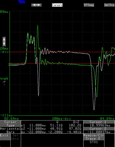
One common measurement technique is time domain reflectometry (TDR). A fast rise time pulse is injected into the differential pair while monitoring the reflected energy. Discontinuities appear as “bumps” in the reflectance waveform. The magnitude indicates the severity of the impedance mismatch.
Another method is to measure the insertion loss (s21) of the differential pair using a vector network analyzer (VNA). This shows the frequency dependence of the loss, which is impacted by impedance discontinuities. Excess insertion loss can point to trouble spots that may need redesign.
Conclusion
Maintaining consistent differential impedance is critical for high-speed PCB designs. While a solid reference plane makes this easier, it’s not always feasible. Disruptions to the reference plane can impact the impedance and cause signal integrity issues.
Careful design techniques such as stitching capacitors, differential cutouts, waveguides, or suspension can mitigate the impact. But there’s no one-size-fits-all solution. Simulation and measurement are key to validating the impedance and identifying any issues.
As data rates continue to rise, differential signaling and Impedance Control will become even more important. PCB designers must understand the principles and tradeoffs involved in breaking the reference plane. With the right tools and techniques, it’s possible to maintain good signal integrity despite these challenges.
Frequently Asked Questions (FAQ)
What is the typical impedance for differential pairs?
Common target impedances are:
– USB: 90 ohms
– PCIe: 100 ohms
– Ethernet: 100 ohms
– HDMI: 100 ohms
How does trace geometry affect differential impedance?
In general:
– Increasing the trace width decreases the impedance
– Increasing the spacing between traces increases the impedance
– Increasing the height above the reference plane decreases the impedance
What is the purpose of stitching capacitors?
Stitching capacitors provide a low-impedance path to reconnect a split reference plane at high frequencies. This helps contain the fields of the differential pair. Typical values range from 100 pF to 100 nF.
When is it okay to suspend differential pairs over a gap?
Suspending the traces may be feasible if:
– The gap is relatively small (less than ~1/10 wavelength)
– The operating frequency is low enough that reflections are tolerable
– Simulation shows no major impact on impedance or insertion loss
What tools are used to simulate differential pairs?
3D full-wave electromagnetic solvers like Ansys HFSS, Keysight EMPro, or CST Studio are commonly used. These tools can model complex structures and predict impedance, insertion loss, and other properties. Many PCB design tools also have built-in 2D field solvers for simple geometries.


Leave a Reply