Introduction to PCB Stackup
Printed Circuit Board (PCB) stackup is a crucial aspect of PCB design that determines the arrangement of copper layers and insulating materials within a PCB. It plays a significant role in the overall performance, reliability, and manufacturability of the final product. In this comprehensive guide, we will dive deep into the world of PCB stackup planning, exploring its fundamentals, best practices, and common challenges.
What is a PCB Stackup?
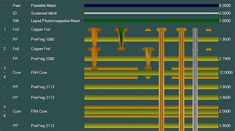
A PCB stackup refers to the arrangement of conductive copper layers and insulating dielectric layers that make up a Multi-Layer PCB. It defines the order in which these layers are stacked and the thickness of each layer. The stackup also specifies the type of materials used for the copper layers and the insulating substrates.
Why is PCB Stackup Planning Important?
Proper PCB stackup planning is essential for several reasons:
-
Signal Integrity: The stackup configuration directly impacts the signal integrity of the PCB. It affects characteristics such as impedance, crosstalk, and electromagnetic interference (EMI).
-
Power Integrity: The placement of power and ground planes in the stackup influences the power delivery network and helps minimize voltage drops and power supply noise.
-
Manufacturability: The choice of materials and the structure of the stackup determine the manufacturability of the PCB. Proper stackup design ensures that the PCB can be fabricated reliably and cost-effectively.
-
Mechanical Strength: The stackup configuration contributes to the mechanical strength and rigidity of the PCB, which is crucial for applications that require robustness and durability.
Factors to Consider in PCB Stackup Planning
When planning a PCB stackup, several key factors need to be considered to ensure optimal performance and manufacturability.
Number of Layers
The number of layers in a PCB stackup depends on the complexity of the design and the routing requirements. Here are some common layer counts and their typical applications:
| Number of Layers | Typical Applications |
|---|---|
| 1 or 2 | Simple circuits, low-density designs |
| 4 | General-purpose designs, moderate complexity |
| 6 or 8 | Complex designs, high-speed digital circuits |
| 10 or more | High-density designs, advanced packaging technologies |
Material Selection
The choice of materials for the copper layers and dielectric substrates is crucial in PCB stackup planning. The most common materials used are:
- FR-4: A glass-reinforced epoxy laminate, widely used for its good mechanical and electrical properties, and cost-effectiveness.
- High-Frequency Laminates: Materials like Rogers RO4000 series or Isola I-Tera are used for high-speed and high-frequency applications due to their low dielectric loss and stable dielectric constant.
- Flexible Materials: Polyimide or polyester-based materials are used for Flexible PCBs that require bending or folding.
Layer Thickness
The thickness of the copper layers and dielectric substrates affects the electrical and mechanical characteristics of the PCB. Typical copper layer thicknesses range from 0.5 oz (17.5 μm) to 2 oz (70 μm), with 1 oz (35 μm) being the most common. The dielectric thickness varies based on the material and the desired impedance of the transmission lines.
Impedance Control
Controlling the impedance of transmission lines is critical for maintaining signal integrity in high-speed designs. The stackup configuration, including the dielectric thickness and the width of the traces, determines the characteristic impedance. Common impedance values are 50Ω for single-ended traces and 100Ω for differential pairs.
Via Configuration
Vias are used to interconnect different layers in a multi-layer PCB. The stackup design should consider the via configuration, including the via size, pad size, and drill size. The choice of via configuration depends on the signal requirements, manufacturing capabilities, and cost considerations.

Best Practices for PCB Stackup Design
To ensure a robust and manufacturable PCB stackup, follow these best practices:
-
Use balanced stackup: Aim for a symmetrical stackup configuration to minimize warpage and improve manufacturability.
-
Separate signal layers: Allocate dedicated layers for signals to reduce crosstalk and EMI.
-
Use ground planes: Incorporate ground planes adjacent to signal layers to provide a low-impedance return path and reduce noise.
-
Optimize power distribution: Place power planes strategically to minimize voltage drops and ensure a stable power supply.
-
Consider via stubs: Minimize via stubs in high-speed designs to reduce reflections and signal integrity issues.
-
Follow manufacturing guidelines: Adhere to the manufacturing capabilities and guidelines provided by the PCB fabricator to ensure manufacturability and reliability.

Common PCB Stackup Configurations
Here are some common PCB stackup configurations for different layer counts:
4-Layer Stackup
| Layer | Material | Thickness | Purpose |
|---|---|---|---|
| 1 | Copper | 1 oz (35 μm) | Signal/Component |
| 2 | FR-4 | 8 mil | Core |
| 3 | Copper | 1 oz (35 μm) | Ground |
| 4 | FR-4 | 47 mil | Prepreg |
| 5 | Copper | 1 oz (35 μm) | Power |
| 6 | FR-4 | 8 mil | Core |
| 7 | Copper | 1 oz (35 μm) | Signal |
6-Layer Stackup
| Layer | Material | Thickness | Purpose |
|---|---|---|---|
| 1 | Copper | 1 oz (35 μm) | Signal/Component |
| 2 | FR-4 | 6 mil | Core |
| 3 | Copper | 1 oz (35 μm) | Ground |
| 4 | FR-4 | 47 mil | Prepreg |
| 5 | Copper | 1 oz (35 μm) | Signal |
| 6 | FR-4 | 47 mil | Prepreg |
| 7 | Copper | 1 oz (35 μm) | Power |
| 8 | FR-4 | 6 mil | Core |
| 9 | Copper | 1 oz (35 μm) | Signal |
8-Layer Stackup
| Layer | Material | Thickness | Purpose |
|---|---|---|---|
| 1 | Copper | 1 oz (35 μm) | Signal/Component |
| 2 | FR-4 | 6 mil | Core |
| 3 | Copper | 1 oz (35 μm) | Ground |
| 4 | FR-4 | 14 mil | Prepreg |
| 5 | Copper | 1 oz (35 μm) | Signal |
| 6 | FR-4 | 47 mil | Core |
| 7 | Copper | 1 oz (35 μm) | Signal |
| 8 | FR-4 | 14 mil | Prepreg |
| 9 | Copper | 1 oz (35 μm) | Power |
| 10 | FR-4 | 6 mil | Core |
| 11 | Copper | 1 oz (35 μm) | Signal |

PCB Stackup Challenges and Solutions
Designing a reliable and manufacturable PCB stackup comes with its own set of challenges. Here are some common challenges and their solutions:
Signal Integrity Issues
High-speed signals are susceptible to signal integrity problems like reflections, crosstalk, and EMI. To mitigate these issues:
- Use controlled impedance traces and maintain consistent impedance throughout the signal path.
- Provide adequate spacing between signal traces to minimize crosstalk.
- Use ground planes and proper grounding techniques to reduce EMI.
Power Integrity Concerns
Insufficient power delivery can lead to voltage drops, power supply noise, and compromised performance. To address power integrity concerns:
- Place power planes close to the components that require a stable power supply.
- Use decoupling capacitors near power pins to reduce high-frequency noise.
- Optimize the placement and sizing of power distribution networks.
Manufacturing Limitations
PCB Fabricators have specific manufacturing capabilities and limitations that need to be considered during stackup design. To ensure manufacturability:
- Communicate with the PCB fabricator early in the design process to understand their capabilities and constraints.
- Follow the manufacturer’s design guidelines for minimum trace widths, spacing, and drill sizes.
- Consider the availability and cost of materials when selecting the stackup configuration.
Conclusion
PCB stackup planning is a critical aspect of PCB design that directly impacts the performance, reliability, and manufacturability of the final product. By understanding the factors involved in stackup design, following best practices, and addressing common challenges, designers can create robust and efficient PCBs that meet the specific requirements of their applications.
Frequently Asked Questions (FAQ)
1. What is the purpose of using a ground plane in a PCB stackup?
A ground plane serves as a low-impedance return path for signals and helps in reducing electromagnetic interference (EMI) and crosstalk. It provides a stable reference for signals and minimizes the loop area, which is crucial for maintaining signal integrity.
2. How does the dielectric constant of the substrate material affect the PCB stackup?
The dielectric constant of the substrate material influences the characteristic impedance of the traces and the propagation velocity of signals. Materials with a higher dielectric constant result in slower signal propagation and require wider traces to achieve the same impedance compared to materials with a lower dielectric constant.
3. What is the significance of via stubs in high-speed PCB designs?
Via stubs are the unused portions of a via that extend beyond the target layer. In high-speed designs, via stubs can cause reflections and degrade signal integrity. It is important to minimize via stubs by using techniques like back-drilling or blind and Buried Vias to improve signal quality.
4. How does the PCB stackup affect the EMI performance of a design?
The PCB stackup plays a crucial role in the EMI performance of a design. Proper stackup configuration, including the placement of ground planes, the use of shielding layers, and the separation of sensitive signals from noisy ones, can help reduce EMI. Additionally, the choice of materials with good high-frequency characteristics can also contribute to better EMI performance.
5. What are the benefits of using a symmetrical stackup configuration?
A symmetrical stackup configuration offers several benefits, including reduced warpage, improved manufacturability, and better signal integrity. By arranging the layers symmetrically around the center of the stackup, the mechanical stresses are balanced, minimizing the chances of warpage during the manufacturing process. Symmetrical stackups also tend to have more predictable electrical characteristics, making it easier to control impedance and maintain signal integrity.


Leave a Reply