Introduction to PCB Design Rules
Printed Circuit Board (PCB) design is a complex process that requires adherence to various design rules to ensure the proper functioning and reliability of the final product. These rules encompass a wide range of aspects, from component placement and routing to signal integrity and manufacturability. By following a set of well-defined PCB design rules, designers can minimize the risk of design issues, reduce the need for costly revisions, and streamline the manufacturing process.
In this article, we will explore 10 essential rules for better data management in PCB design. These rules will help you avoid common design issues, improve the quality of your PCBs, and ultimately lead to more successful projects.
Rule 1: Maintain Consistent and Accurate Design Data
One of the most crucial aspects of PCB design is maintaining consistent and accurate design data throughout the entire process. This includes schematic symbols, footprints, component information, and design constraints. Inconsistencies or errors in design data can lead to a range of issues, such as incorrect component placement, routing difficulties, and manufacturing problems.
To avoid these issues, consider the following best practices:
- Use a centralized library management system to ensure all team members have access to the most up-to-date component information.
- Regularly review and update your design data to maintain accuracy and consistency.
- Implement version control to track changes and allow for easy rollbacks if necessary.
- Establish a clear naming convention for components, nets, and other design elements to avoid confusion and errors.
| Data Type | Best Practices |
|---|---|
| Schematic Symbols | – Use consistent naming conventions – Ensure accurate pin assignments – Include relevant component information |
| Footprints | – Verify dimensions and pad sizes – Include appropriate clearances and tolerances – Use standardized footprint naming |
| Component Information | – Maintain up-to-date datasheets and specifications – Include relevant parameters (e.g., voltage, current, power ratings) – Use consistent units and formatting |
| Design Constraints | – Define clear rules for routing, spacing, and sizing – Communicate constraints to all team members – Regularly review and update constraints as needed |
By adhering to these best practices and maintaining consistent and accurate design data, you can minimize the risk of design issues and ensure a smoother PCB design process.

Rule 2: Follow Manufacturer’s Design Guidelines
Each PCB manufacturer has its own set of design guidelines that designers must follow to ensure the manufacturability and reliability of their boards. These guidelines cover various aspects of PCB design, such as minimum trace widths, spacing requirements, hole sizes, and copper weights.
Failing to adhere to the manufacturer’s design guidelines can result in a range of issues, including:
- Difficulty in manufacturing the PCB
- Increased production costs
- Reduced reliability and performance of the final product
To avoid these problems, take the following steps:
- Obtain the manufacturer’s design guidelines early in the design process.
- Carefully review the guidelines and ensure your design complies with all requirements.
- Communicate the guidelines to all team members involved in the design process.
- Regularly check your design against the guidelines to catch any violations or discrepancies.
| Aspect | Typical Guideline | Potential Issues |
|---|---|---|
| Minimum Trace Width | 0.1 mm (4 mil) | – Increased resistance – Manufacturing difficulties |
| Minimum Spacing | 0.1 mm (4 mil) | – Short circuits – Signal integrity issues |
| Minimum Hole Size | 0.2 mm (8 mil) | – Difficulty in drilling – Reduced reliability |
| Copper Weight | 1 oz (35 µm) | – Insufficient current carrying capacity – Manufacturability issues |
By following the manufacturer’s design guidelines closely, you can ensure your PCB design is optimized for manufacturability and reliability, ultimately leading to a more successful project outcome.

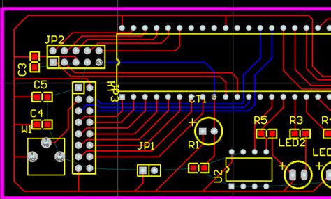
Rule 3: Use Appropriate Component Placement and Orientation
Proper component placement and orientation are essential for ensuring the optimal performance and reliability of your PCB. Poor placement can lead to signal integrity issues, thermal problems, and manufacturing difficulties.
Consider the following guidelines when placing components on your PCB:
- Group related components together to minimize trace lengths and improve signal integrity.
- Place sensitive components, such as high-speed devices or analog circuits, away from potential sources of interference (e.g., power supplies, digital circuits).
- Orient components to facilitate efficient routing and minimize the number of vias required.
- Ensure adequate spacing between components to allow for proper soldering and heat dissipation.
- Consider the mechanical constraints of the enclosure or system in which the PCB will be used.
Here’s an example of how component placement can impact trace lengths:
| Placement Strategy | Average Trace Length |
|---|---|
| Grouped by function | 25 mm |
| Randomly dispersed | 45 mm |
By grouping related components together, you can significantly reduce the average trace length, leading to improved signal integrity and reduced electromagnetic interference (EMI).
Proper component orientation is also crucial for manufacturability. Ensure that all components are oriented in a manner that allows for easy assembly and soldering. Avoid placing components too close to the edge of the board or in hard-to-reach areas, as this can make the assembly process more challenging and increase the risk of defects.

Rule 4: Optimize Signal Routing and Layer Stackup
Signal routing and layer stackup are critical factors in ensuring the proper functioning and reliability of your PCB. Poor routing or an inadequate layer stackup can lead to signal integrity issues, crosstalk, and EMI problems.
To optimize your signal routing and layer stackup, consider the following best practices:
- Use a consistent routing strategy, such as orthogonal or 45-degree routing, to minimize trace lengths and reduce the risk of signal integrity issues.
- Maintain appropriate trace widths and spacing based on the signal requirements and the manufacturer’s guidelines.
- Use ground planes and power planes to provide a low-impedance return path for signals and minimize EMI.
- Carefully plan your layer stackup to ensure proper signal referencing and minimize crosstalk between layers.
- Use appropriate Via sizes and placement to minimize the impact on signal integrity and manufacturability.
Here’s an example of a well-designed 4-layer PCB Stackup:
| Layer | Purpose |
|---|---|
| Top | Signal routing, components |
| Inner 1 | Ground plane |
| Inner 2 | Power plane |
| Bottom | Signal routing, components |
By using dedicated ground and power planes, you can provide a stable reference for your signals and reduce the risk of EMI and crosstalk. This stackup also allows for efficient signal routing on the top and bottom layers while minimizing the need for vias.
When routing signals, pay close attention to high-speed or sensitive traces. Use techniques such as impedance matching, length matching, and differential pair routing to maintain signal integrity and minimize reflections or crosstalk.
Rule 5: Implement Robust Power Distribution Network (PDN)
A well-designed power distribution network (PDN) is essential for ensuring the stable and reliable operation of your PCB. A poor PDN can lead to voltage fluctuations, noise, and other power-related issues that can compromise the performance and reliability of your design.
To implement a robust PDN, consider the following guidelines:
- Use appropriate copper weights and trace widths to ensure adequate current carrying capacity and minimize voltage drops.
- Place Decoupling capacitors close to power pins of ICs to suppress high-frequency noise and provide local energy storage.
- Use separate power planes for analog and digital circuits to minimize crosstalk and noise coupling.
- Implement proper grounding techniques, such as star grounding or grounding grids, to provide a low-impedance return path for signals.
- Consider the use of power integrity simulation tools to analyze and optimize your PDN design.
Here’s an example of how decoupling capacitor placement can impact power supply noise:
| Capacitor Placement | Power Supply Noise |
|---|---|
| Close to IC power pins | 10 mV |
| Randomly dispersed | 50 mV |
By placing decoupling capacitors close to the power pins of ICs, you can significantly reduce power supply noise and ensure a more stable power delivery to your components.
When designing your PDN, also consider the power requirements of your components and the expected operating conditions. Use Voltage Regulators and power management ICs as necessary to provide stable and regulated power supplies to your circuits.
Rule 6: Conduct Thorough Design Reviews and Simulations
Conducting thorough design reviews and simulations is crucial for catching potential issues early in the design process and ensuring the overall quality and reliability of your PCB.
Design reviews should involve a cross-functional team, including engineers, PCB designers, and manufacturing experts. During these reviews, focus on the following aspects:
- Schematic accuracy and completeness
- Component selection and availability
- Footprint and layout correctness
- Compliance with design rules and manufacturing guidelines
- Signal integrity and power integrity considerations
In addition to design reviews, use simulation tools to analyze and optimize your PCB design. Some common simulations include:
- Signal integrity simulations: Analyze the quality of high-speed signals and identify potential issues such as reflections, crosstalk, and EMI.
- Power integrity simulations: Evaluate the performance of your PDN and identify areas for improvement, such as decoupling capacitor placement or plane resonances.
- Thermal simulations: Assess the thermal performance of your PCB and ensure that components operate within their specified temperature ranges.
| Simulation Type | Potential Issues Identified |
|---|---|
| Signal Integrity | – Reflections – Crosstalk – EMI |
| Power Integrity | – Voltage drops – Plane resonances – Decoupling issues |
| Thermal | – Overheating components – Insufficient heat dissipation |
By conducting thorough design reviews and simulations, you can identify and address potential issues early in the design process, ultimately leading to a more robust and reliable PCB.
Rule 7: Optimize for Manufacturability and Assembly
Designing your PCB with manufacturability and assembly in mind can help you avoid potential issues during production and ensure a more cost-effective and efficient process.
Consider the following guidelines to optimize your PCB design for manufacturability and assembly:
- Follow the manufacturer’s design guidelines for minimum trace widths, spacing, hole sizes, and other parameters.
- Use standard component package sizes and footprints whenever possible to simplify sourcing and assembly.
- Provide adequate clearances around components and connectors to allow for easy soldering and inspection.
- Use surface mount devices (SMDs) whenever possible to reduce drilling costs and improve assembly efficiency.
- Consider the use of panelization to maximize material utilization and reduce fabrication costs.
Here’s an example of how using standard component packages can impact assembly costs:
| Component Package | Relative Assembly Cost |
|---|---|
| Standard (e.g., 0805, SOIC) | 1x |
| Custom or specialty packages | 2x to 5x |
By using standard component packages, you can significantly reduce assembly costs and simplify the sourcing process.
In addition to these guidelines, communicate closely with your manufacturing partners throughout the design process. They can provide valuable insights and feedback on your design, helping you identify potential manufacturability issues early on.
Rule 8: Document and Communicate Design Intent
Clear documentation and communication of your design intent are essential for ensuring that all stakeholders, including engineers, PCB designers, and manufacturing partners, have a shared understanding of the project goals and requirements.
To effectively document and communicate your design intent, consider the following practices:
- Create a comprehensive design specification document that outlines the key requirements, constraints, and objectives of your PCB design.
- Use clear and consistent naming conventions for components, nets, and other design elements to avoid confusion and errors.
- Provide detailed component information, including datasheets, application notes, and any special handling or assembly requirements.
- Include appropriate design notes and comments within your schematic and layout files to clarify design decisions and provide guidance for future modifications.
- Regularly communicate with all stakeholders to ensure alignment and address any questions or concerns.
| Documentation Type | Key Elements |
|---|---|
| Design Specification | – Functional requirements – Performance targets – Environmental constraints – Regulatory compliance |
| Component Information | – Datasheets – Application notes – Special handling or assembly requirements |
| Design Notes | – Design decisions – Guidance for future modifications – Clarification of design intent |
By thoroughly documenting and communicating your design intent, you can minimize the risk of misunderstandings, errors, and delays throughout the PCB design and manufacturing process.
Rule 9: Implement Revision Control and Change Management
Implementing effective revision control and change management processes is crucial for maintaining the integrity of your PCB design data and ensuring that all stakeholders are working with the most up-to-date information.
Consider the following best practices for revision control and change management:
- Use a version control system (VCS) to track changes to your design files, including schematics, layouts, and documentation.
- Establish a clear and consistent naming convention for design revisions and releases.
- Implement a formal change request process to ensure that all modifications to the design are properly reviewed, approved, and documented.
- Maintain a detailed change log that records the nature, reason, and impact of each design change.
- Regularly communicate design changes to all stakeholders to ensure everyone is working with the most current information.
Here’s an example of a simple revision naming convention:
| Revision | Description |
|---|---|
| A1 | Initial design release |
| A2 | Minor design changes |
| B1 | Major design changes or additions |
| C1 | Final design release for production |
By using a clear and consistent naming convention, you can easily track the progress of your design and ensure that all stakeholders are aware of the current revision level.
Effective change management also involves carefully assessing the impact of each proposed design change. Consider the following factors when evaluating a change request:
- Reason for the change (e.g., performance improvement, cost reduction, manufacturability)
- Impact on schedule and budget
- Potential risks or unintended consequences
- Compatibility with existing design elements and requirements
By implementing robust revision control and change management processes, you can maintain the integrity of your PCB design data, minimize the risk of errors or confusion, and ensure a more efficient and successful project outcome.
Rule 10: Foster Collaboration and Continuous Improvement
Fostering a culture of collaboration and continuous improvement is essential for driving innovation, reducing design issues, and ensuring the long-term success of your PCB design projects.
To promote collaboration and continuous improvement, consider the following strategies:
- Encourage open communication and knowledge sharing among team members, including engineers, PCB designers, and manufacturing partners.
- Regularly conduct post-project reviews to identify successes, challenges, and areas for improvement.
- Invest in ongoing training and education to keep team members up-to-date with the latest PCB design techniques, tools, and best practices.
- Establish a centralized knowledge base or design library to capture and share lessons learned, best practices, and design templates.
- Foster a culture of experimentation and innovation, encouraging team members to explore new ideas and approaches to PCB design.
| Initiative | Benefits |
|---|---|
| Post-Project Reviews | – Identify areas for improvement – Share lessons learned – Celebrate successes |
| Ongoing Training | – Stay current with industry trends – Improve design skills and knowledge – Drive innovation and efficiency |
| Centralized Knowledge Base | – Capture and share best practices – Reduce duplicated effort – Facilitate onboarding of new team members |
By fostering a culture of collaboration and continuous improvement, you can create an environment that encourages learning, innovation, and the pursuit of excellence in PCB design.
Frequently Asked Questions (FAQ)
-
Q: What are the most common PCB design issues, and how can I avoid them?
A: Common PCB design issues include signal integrity problems, power distribution issues, and manufacturability challenges. To avoid these issues, follow best practices such as proper component placement, optimized signal routing, robust power distribution, and adherence to manufacturer’s design guidelines. -
Q: How can I ensure my PCB design is optimized for manufacturability?
A: To optimize your PCB design for manufacturability, follow the manufacturer’s design guidelines for minimum trace widths, spacing, hole sizes, and other parameters. Use standard component package sizes and footprints whenever possible, provide adequate clearances around components, and consider the use of panelization to maximize material utilization. -
Q: What are the benefits of conducting thorough design reviews and simulations?
A: Conducting thorough design reviews and simulations helps catch potential issues early in the design process, ensuring the overall quality and reliability of your PCB. Design reviews involve a cross-functional team to assess schematic accuracy, component selection, layout correctness, and compliance with design rules. Simulations, such as signal integrity, power integrity, and thermal simulations, help identify and address specific performance issues. -
Q: How can I effectively manage design changes and revisions?
A: To effectively manage design changes and revisions, use a version control system (VCS) to track changes to your design files. Establish a clear and consistent naming convention for design revisions and releases, and implement a formal change request process to ensure that all modifications


Leave a Reply