Introduction to Solder Stencils
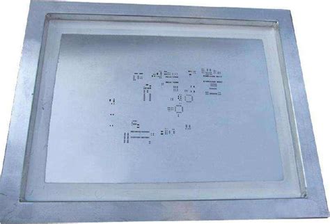
Solder stencils are an essential tool in the world of Electronic Assembly, particularly in surface mount technology (SMT). These thin metal sheets, typically made from stainless steel or nickel, feature a precise pattern of apertures that correspond to the pads on a printed circuit board (PCB). The stencil is used to apply solder paste onto the PCB, ensuring that the correct amount of paste is deposited in the right locations. This process is crucial for achieving reliable and consistent solder joints during the reflow soldering process.
In this article, we will explore the various aspects of making solder paste stencils, including the materials and techniques used, design considerations, and best practices for achieving optimal results.
The Importance of Solder Stencils in PCB Assembly
Advantages of Using Solder Stencils
Solder stencils offer several key advantages in the PCB assembly process:
- Precision: Stencils ensure that the solder paste is applied accurately and consistently, minimizing the risk of shorts, bridges, or insufficient solder joints.
- Speed: Using a stencil to apply solder paste is much faster than manual methods, making it suitable for high-volume production.
- Repeatability: Stencils allow for a highly repeatable process, ensuring that each PCB receives the same amount of solder paste in the correct locations.
The Role of Solder Stencils in SMT Assembly
In surface mount technology (SMT) assembly, solder stencils play a critical role in the following steps:
- Solder paste application: The stencil is placed over the PCB, and solder paste is applied using a squeegee or automated printer.
- Component placement: After the solder paste is applied, SMT components are placed onto the PCB, with their leads or terminals aligned with the solder paste deposits.
- Reflow soldering: The PCB with components is then heated in a reflow oven, causing the solder paste to melt and form a strong bond between the components and the PCB Pads.

Solder Stencil Materials and Fabrication Methods
Common Materials Used for Solder Stencils
Solder stencils are typically made from one of two materials:
- Stainless steel: This is the most common material for solder stencils due to its durability, stability, and resistance to wear and corrosion. Stainless steel stencils are available in various thicknesses, typically ranging from 0.1 mm to 0.2 mm (4 to 8 mils).
- Nickel: Nickel stencils are an alternative to stainless steel and offer similar properties. They are sometimes preferred for their non-magnetic properties and resistance to oxidation.
Solder Stencil Fabrication Techniques
There are several methods used to fabricate solder stencils, each with its own advantages and limitations:
- Laser cutting: This is the most common method for creating solder stencils. A high-powered laser is used to cut the aperture pattern into the metal sheet, offering high precision and fast turnaround times.
- Chemical etching: In this process, a photoresist is applied to the metal sheet, and the aperture pattern is developed using UV light. The exposed areas are then etched away using a chemical solution, leaving the desired stencil pattern.
- Electroforming: This method involves growing a metal layer (typically nickel) onto a master pattern using an electroplating process. The resulting stencil is then peeled away from the master, offering high accuracy and the ability to create fine details.
| Fabrication Method | Advantages | Disadvantages |
|---|---|---|
| Laser cutting | High precision, fast turnaround | Limited to certain materials, higher cost |
| Chemical etching | Lower cost, suitable for large apertures | Lower precision, slower turnaround |
| Electroforming | High accuracy, fine detail capability | Higher cost, slower turnaround |

Designing Solder Stencils
Aperture Design Considerations
When designing solder stencils, several key factors must be considered to ensure optimal solder paste deposition:
- Aperture size: The size of the apertures should be based on the size of the PCB pads and the desired amount of solder paste. Typically, the aperture size is slightly larger than the pad size to allow for some tolerance.
- Aperture shape: The shape of the apertures can affect the solder paste release and the resulting solder joint. Common aperture shapes include square, circular, and home plate (a combination of square and circular).
- Aperture orientation: The orientation of the apertures should be aligned with the PCB pads to ensure proper solder paste deposition and component placement.
Stencil Thickness and Its Impact on Solder Paste Deposition
The thickness of the solder stencil plays a significant role in the amount of solder paste deposited onto the PCB. Thicker stencils will deposit more paste, while thinner stencils will deposit less. The optimal stencil thickness depends on several factors, including:
- Component pitch: Finer pitch components require thinner stencils to prevent bridging and shorts.
- Solder paste type: Different solder paste formulations may require different stencil thicknesses for optimal performance.
- PCB Surface Finish: The surface finish of the PCB can affect the solder paste adhesion and may require adjustments to the stencil thickness.
Common stencil thicknesses and their applications:
| Stencil Thickness | Application |
|---|---|
| 0.1 mm (4 mils) | Fine pitch components (0.4 mm pitch or less) |
| 0.15 mm (6 mils) | Standard SMT components (0.5 mm to 0.8 mm pitch) |
| 0.2 mm (8 mils) | Larger SMT components and through-hole components |
CAD Tools and File Formats for Solder Stencil Design
Solder stencils are typically designed using computer-aided design (CAD) tools, which allow for precise control over the aperture size, shape, and placement. Some common CAD tools used for stencil design include:
- Gerber files: This is the most common file format for PCB and stencil design, and it is widely supported by CAD tools and fabrication houses.
- ODB++: This is an intelligent CAD format that includes additional information beyond the basic aperture data, such as component placement and orientation.
- DXF: This is a common CAD file format that can be used for solder stencil design, although it is less widely supported than Gerber files.
When designing solder stencils, it is essential to work closely with the fabrication house to ensure that the design files are compatible with their manufacturing processes and equipment.

Solder Stencil Printing Process
Setting Up the Solder Paste Printer
Before printing solder paste onto the PCB, the solder paste printer must be properly set up and calibrated. This involves several key steps:
- Mounting the stencil: The solder stencil is mounted onto the printer’s frame, ensuring that it is taut and free from wrinkles or distortions.
- Aligning the PCB: The PCB is placed on the printer’s bed and aligned with the stencil using fiducial marks or automatic vision systems.
- Adjusting the printer settings: The printer’s parameters, such as squeegee pressure, speed, and separation distance, are adjusted based on the solder paste type, stencil thickness, and PCB characteristics.
Solder Paste Printing Techniques
There are two main techniques used for printing solder paste through a stencil:
- Manual printing: In this method, a handheld squeegee is used to manually spread the solder paste across the stencil, forcing it through the apertures and onto the PCB. This technique is suitable for low-volume production or prototyping.
- Automated printing: Automated solder paste printers use a motorized squeegee and a precise control system to apply the solder paste consistently and accurately. This method is preferred for high-volume production and ensures better repeatability and quality control.
Inspection and Quality Control
After the solder paste is printed onto the PCB, it is essential to inspect the result to ensure that the paste has been deposited correctly. This can be done using several methods:
- Visual inspection: A trained operator can visually inspect the PCB for any obvious defects, such as missing or excessive solder paste, bridges, or smears.
- Automated optical inspection (AOI): AOI systems use high-resolution cameras and image processing algorithms to automatically detect and analyze solder paste deposits, identifying any defects or irregularities.
- Solder paste inspection (SPI): SPI systems use 3D measurement techniques, such as laser triangulation or structured light, to assess the volume, height, and shape of the solder paste deposits, providing quantitative data for quality control.
By implementing a robust inspection and quality control process, manufacturers can identify and correct any issues with the solder paste printing process, ensuring high-quality PCB assembly.
Maintaining and Troubleshooting Solder Stencils
Cleaning and Storage Best Practices
To ensure consistent performance and long life, solder stencils must be properly cleaned and stored. Some best practices include:
- Regular cleaning: Solder stencils should be cleaned after every use to remove any residual solder paste or debris. This can be done using a variety of methods, such as manual wiping with solvents, ultrasonic cleaning, or automated stencil cleaners.
- Proper storage: When not in use, solder stencils should be stored in a clean, dry environment, away from any sources of contamination or damage. Stencils should be stored flat or hung vertically to prevent warping or distortion.
- Handling with care: Solder stencils are delicate and can be easily damaged by improper handling. Operators should use gloves when handling stencils and avoid touching the apertures or the printing surface.
Troubleshooting Common Solder Stencil Issues
Despite best efforts, issues can sometimes arise with solder stencils. Some common problems and their solutions include:
- Clogged apertures: If solder paste becomes stuck in the stencil apertures, it can cause inconsistent or incomplete paste deposition. This can be addressed by thoroughly cleaning the stencil or using a stencil with a non-stick coating.
- Stencil warping: If a stencil becomes warped or distorted, it can lead to uneven solder paste deposition and poor print quality. This can be prevented by proper storage and handling, or by using a thicker or more rigid stencil material.
- Poor paste release: If the solder paste does not release cleanly from the stencil apertures, it can result in incomplete or inconsistent deposits. This can be improved by adjusting the stencil aperture design, using a different solder paste formulation, or optimizing the printer settings.
By understanding and addressing these common issues, manufacturers can maintain high-quality solder paste printing and ensure reliable PCB assembly.
Frequently Asked Questions (FAQ)
- What is the difference between solder paste and solder stencils?
-
Solder paste is a mixture of tiny solder particles suspended in a flux medium, used for bonding components to PCBs. Solder stencils are thin metal sheets with a precise pattern of apertures, used to apply solder paste onto PCBs in the correct locations and quantities.
-
Can solder stencils be reused?
-
Yes, solder stencils can be reused many times with proper cleaning and maintenance. However, over time, the stencil apertures may wear or become damaged, requiring the stencil to be replaced.
-
What is the typical lifespan of a solder stencil?
-
The lifespan of a solder stencil depends on various factors, such as the material, thickness, usage frequency, and maintenance. With proper care, a stainless steel stencil can last for thousands of prints, while a nickel stencil may last even longer. However, stencils should be regularly inspected for wear and replaced as necessary.
-
How do I choose the right solder stencil thickness?
-
The optimal solder stencil thickness depends on the specific requirements of the PCB assembly, including the component pitch, solder paste type, and PCB surface finish. As a general rule, finer pitch components require thinner stencils (0.1 mm or 4 mils), while larger components and through-hole parts can use thicker stencils (0.15 mm to 0.2 mm, or 6 to 8 mils).
-
Can solder stencils be customized for specific PCB designs?
- Yes, solder stencils are typically custom-made for each specific PCB design. The stencil aperture pattern is based on the PCB layout and can be optimized for the desired solder paste deposition. CAD tools and standard file formats, such as Gerber files, are used to create custom stencil designs that match the PCB pads and component locations.
Conclusion
Solder stencils are a critical tool in the world of PCB assembly, enabling the precise and consistent application of solder paste for surface mount components. By understanding the materials, fabrication methods, design considerations, and best practices involved in making and using solder stencils, manufacturers can achieve high-quality, reliable PCB assemblies.
Proper selection of stencil materials, thicknesses, and aperture designs, combined with optimized printer setup and thorough inspection and maintenance, can help ensure that solder paste is deposited accurately and efficiently. This, in turn, leads to better solder joint formation, fewer defects, and higher yields in the PCB assembly process.
As electronics continue to evolve, with ever-smaller components and more complex designs, the importance of solder stencils will only continue to grow. By staying up-to-date with the latest technologies and best practices in solder stencil manufacturing and use, PCB assembly professionals can meet the challenges of today’s demanding electronics landscape and deliver high-quality, reliable products to their customers.


Leave a Reply