What is PCB Visualizer?
PCB Visualizer is a powerful software tool designed to help engineers, designers, and manufacturers create, analyze, and optimize printed circuit board (PCB) designs. It provides a user-friendly interface that allows users to visualize and interact with their PCB designs in a 3D environment, making it easier to identify potential issues and make necessary modifications before the manufacturing process begins.
Key Features of PCB Visualizer
| Feature | Description |
|---|---|
| 3D Visualization | Allows users to view their PCB designs in a realistic 3D environment, providing a better understanding of the board’s layout and components. |
| Real-time Collaboration | Enables team members to work together on PCB designs in real-time, regardless of their location, improving collaboration and productivity. |
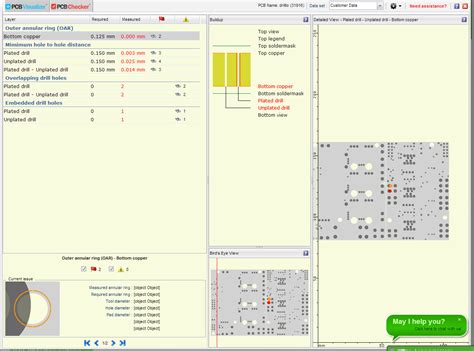
| Design Rule Checking (DRC) | Automatically checks the PCB design for potential errors or violations of design rules, helping to ensure the manufacturing process goes smoothly. |
| Bill of Materials (BOM) Management | Helps users manage and organize the list of components required for their PCB design, making it easier to track and order necessary parts. |
| Integration with Popular CAD Tools | Seamlessly integrates with popular CAD tools such as Altium Designer, Eagle, and KiCad, allowing users to import and export their designs with ease. |
Why Use PCB Visualizer?
Improved Design Accuracy
One of the primary benefits of using PCB Visualizer is the improved accuracy of PCB designs. By providing a 3D visualization of the board, users can easily identify potential issues such as component clearance, trace routing, and thermal management. This allows for more precise designs and reduces the risk of errors during the manufacturing process.
Enhanced Collaboration
PCB Visualizer’s real-time collaboration features enable team members to work together on PCB designs, regardless of their location. This improves communication and collaboration among team members, leading to more efficient and effective design processes.
Faster Time to Market
By streamlining the PCB design process and reducing the risk of errors, PCB Visualizer helps companies bring their products to market faster. The software’s automated design rule checking and BOM management features help to ensure that designs are ready for manufacturing, minimizing delays and reducing the need for costly revisions.
Cost Savings
Using PCB Visualizer can lead to significant cost savings for companies. By identifying and addressing potential issues early in the design process, companies can avoid expensive manufacturing errors and redesigns. Additionally, the software’s optimization features can help to reduce the overall cost of PCB Production by minimizing the use of materials and improving manufacturing efficiency.

Applications of PCB Visualizer
PCB Visualizer is used in a wide range of industries and applications, including:
- Consumer electronics
- Automotive electronics
- Medical devices
- Aerospace and defense
- Industrial automation
- Internet of Things (IoT) devices
Consumer Electronics
In the consumer electronics industry, PCB Visualizer is used to design and optimize PCBs for products such as smartphones, tablets, laptops, and wearables. The software’s 3D visualization and design rule checking features help to ensure that these complex designs meet the necessary performance and reliability requirements.
Automotive Electronics
PCB Visualizer is also widely used in the automotive industry, where the demand for advanced electronic systems continues to grow. The software is used to design and optimize PCBs for applications such as infotainment systems, driver assistance systems, and vehicle control units.
Medical Devices
In the medical device industry, PCB Visualizer is used to design and optimize PCBs for a wide range of applications, including diagnostic equipment, monitoring systems, and implantable devices. The software’s ability to ensure accurate and reliable designs is critical in this industry, where patient safety is of the utmost importance.

How PCB Visualizer Works
PCB Visualizer works by importing PCB design files from popular CAD tools such as Altium Designer, Eagle, and KiCad. Once the design is imported, users can view and interact with the board in a realistic 3D environment.
The software automatically checks the design for potential errors or violations of design rules, such as minimum trace widths, clearances, and drill sizes. If any issues are identified, users can make the necessary modifications directly within PCB Visualizer.
PCB Visualizer also provides a range of tools for optimizing the design, such as automatic component placement and trace routing. These features help to minimize the overall size of the board and improve its performance and reliability.
Integrating PCB Visualizer into the Design Workflow
To get the most out of PCB Visualizer, it’s important to integrate the software into the overall PCB design workflow. This typically involves the following steps:
- Design the initial PCB layout using a CAD tool such as Altium Designer or Eagle.
- Import the design into PCB Visualizer for 3D visualization and analysis.
- Use PCB Visualizer’s design rule checking and optimization features to identify and address any potential issues.
- Collaborate with team members using PCB Visualizer’s real-time collaboration features.
- Export the optimized design back to the original CAD tool for final refinements and manufacturing.
By following this workflow, companies can take full advantage of PCB Visualizer’s capabilities and streamline their PCB design processes.

Future of PCB Visualizer
As the demand for advanced electronic systems continues to grow, the role of PCB Visualizer in the design and manufacturing process is likely to become even more important. In the coming years, we can expect to see continued development and innovation in the software, with new features and capabilities being added to meet the evolving needs of the industry.
Some potential areas of development for PCB Visualizer include:
- Integration with advanced manufacturing technologies such as 3D printing and flexible electronics.
- Improved simulation and analysis capabilities for more accurate performance predictions.
- Enhanced collaboration features for better communication and coordination among team members.
- Increased automation and optimization capabilities to further streamline the design process.
As these developments take place, PCB Visualizer is likely to become an even more essential tool for companies looking to stay competitive in the fast-paced world of electronic product design and manufacturing.
Conclusion
PCB Visualizer is a powerful software tool that is transforming the way companies design and manufacture electronic products. By providing a range of features for 3D visualization, collaboration, design rule checking, and optimization, the software helps to improve design accuracy, reduce errors, and bring products to market faster.
As the demand for advanced electronic systems continues to grow, the role of PCB Visualizer in the design and manufacturing process is likely to become even more important. By staying up-to-date with the latest developments in the software and integrating it into their overall design workflows, companies can position themselves for success in the competitive world of electronic product design and manufacturing.
Frequently Asked Questions (FAQ)
-
What is PCB Visualizer used for?
PCB Visualizer is used to create, analyze, and optimize printed circuit board (PCB) designs. It provides a 3D visualization of the board, allowing users to identify potential issues and make necessary modifications before the manufacturing process begins. -
What industries use PCB Visualizer?
PCB Visualizer is used in a wide range of industries, including consumer electronics, automotive electronics, medical devices, aerospace and defense, industrial automation, and Internet of Things (IoT) devices. -
How does PCB Visualizer improve collaboration among team members?
PCB Visualizer’s real-time collaboration features enable team members to work together on PCB designs, regardless of their location. This improves communication and coordination among team members, leading to more efficient and effective design processes. -
What are some of the key features of PCB Visualizer?
Some of the key features of PCB Visualizer include 3D visualization, real-time collaboration, design rule checking (DRC), bill of materials (BOM) management, and integration with popular CAD tools. -
How can companies integrate PCB Visualizer into their overall design workflows?
To integrate PCB Visualizer into their overall design workflows, companies typically follow these steps: - Design the initial PCB layout using a CAD tool.
- Import the design into PCB Visualizer for 3D visualization and analysis.
- Use PCB Visualizer’s design rule checking and optimization features to identify and address any potential issues.
- Collaborate with team members using PCB Visualizer’s real-time collaboration features.
- Export the optimized design back to the original CAD tool for final refinements and manufacturing.


Leave a Reply