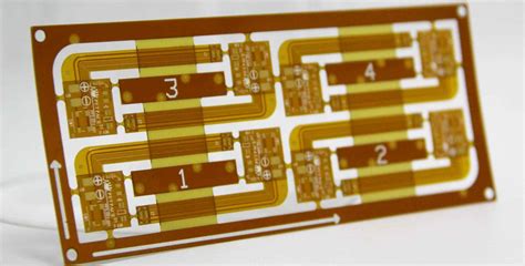
What is SEMI-FLEX PCB?
SEMI-Flex PCBs, also known as semi-flexible printed circuit boards, are a type of PCB that combines the properties of both rigid and flexible PCBs. They consist of rigid sections connected by flexible sections, allowing for a certain degree of flexibility while maintaining the stability and durability of rigid PCBs. This unique combination makes SEMI-FLEX PCBs suitable for a wide range of applications, particularly in industries where space constraints and the need for flexibility are critical factors.
Advantages of SEMI-FLEX PCBs
-
Space-saving design: SEMI-FLEX PCBs can be folded, bent, or twisted to fit into tight spaces, making them ideal for compact electronic devices.
-
Improved reliability: The combination of rigid and flexible sections reduces the risk of connection failures and enhances the overall reliability of the circuit.
-
Reduced assembly costs: SEMI-FLEX PCBs eliminate the need for additional connectors and wiring, simplifying the assembly process and reducing costs.
-
Enhanced signal integrity: The shorter signal paths and reduced number of connections in SEMI-FLEX PCBs minimize signal loss and interference.
-
Increased design flexibility: SEMI-FLEX PCBs allow for more creative and innovative product designs, as they can be shaped to fit unique form factors.
SEMI-FLEX PCB Structure and Materials
Layers in a SEMI-FLEX PCB
A typical SEMI-FLEX PCB consists of the following layers:
| Layer | Description |
|---|---|
| Coverlay | Protective layer on the outer surface of the flexible section |
| Copper | Conductive layer for Circuit Traces |
| Adhesive | Bonds the copper layer to the substrate |
| Substrate (Flexible) | Flexible insulating material, typically polyimide |
| Substrate (Rigid) | Rigid insulating material, typically FR-4 |
Common Materials Used in SEMI-FLEX PCBs
-
Polyimide: A flexible, heat-resistant material used as the substrate for the flexible sections of the PCB.
-
FR-4: A rigid, glass-reinforced epoxy laminate used as the substrate for the rigid sections of the PCB.
-
Copper: The conductive material used for circuit traces and pads.
-
Coverlay: A protective layer, typically made of polyimide or solder mask, applied to the outer surface of the flexible sections.

SEMI-FLEX PCB Design Considerations
Bend Radius
The bend radius is a critical factor in SEMI-FLEX PCB design, as it determines the minimum allowable radius of curvature for the flexible sections without causing damage or affecting performance. The minimum bend radius depends on factors such as the thickness of the flexible substrate, copper weight, and the number of layers.
Stiffeners
Stiffeners are used to reinforce specific areas of the SEMI-FLEX PCB, particularly the transition points between rigid and flexible sections. They help to distribute stress evenly and prevent excessive bending or twisting, which could lead to circuit damage.
Copper Weight
The copper weight, or thickness, used in SEMI-FLEX PCBs should be carefully considered. Thinner copper weights are more flexible but have lower current-carrying capacity, while thicker copper weights offer better electrical performance but reduced flexibility.
Trace Width and Spacing
Trace width and spacing should be optimized to ensure proper signal integrity and minimize the risk of short circuits or signal interference. In general, wider traces and greater spacing are recommended for the flexible sections to accommodate bending and movement.

SEMI-FLEX PCB Manufacturing Process
The manufacturing process for SEMI-FLEX PCBs involves several key steps:
-
Design and Layout: The PCB design is created using CAD software, taking into account the specific requirements for the rigid and flexible sections.
-
Material Selection: The appropriate materials for the substrate, copper, and coverlay are chosen based on the application and performance requirements.
-
Lamination: The copper layers are bonded to the substrate using heat and pressure, creating a multilayer structure.
-
Drilling: Holes are drilled through the PCB for vias, component mounting, and other features.
-
Patterning: The copper layers are selectively etched to create the desired circuit pattern.
-
Surface Finishing: A protective surface finish, such as ENIG (Electroless Nickel Immersion Gold) or OSP (Organic Solderability Preservative), is applied to the exposed copper surfaces.
-
Solder Mask Application: A solder mask is applied to the outer layers of the PCB to protect the circuitry and prevent short circuits.
-
Silkscreen Printing: Text, logos, and other markings are printed onto the PCB surface using silkscreen printing.
-
Cutting and Routing: The PCB panel is cut and routed to the desired shape and size, separating the individual PCBs.
-
Quality Control: The finished PCBs undergo thorough inspection and testing to ensure they meet the required specifications and performance standards.

Applications of SEMI-FLEX PCBs
SEMI-FLEX PCBs find applications in various industries and products, including:
-
Consumer Electronics: Smartphones, tablets, wearables, and other compact devices.
-
Automotive: In-vehicle infotainment systems, dashboard displays, and sensors.
-
Medical Devices: Implantable devices, diagnostic equipment, and patient monitoring systems.
-
Aerospace and Defense: Avionics, satellite systems, and military communication devices.
-
Industrial Equipment: Robotics, automation systems, and machine Control Panels.
SEMI-FLEX PCB Assembly Services
Many PCB manufacturers offer SEMI-FLEX PCB assembly services to help customers bring their products to market more efficiently. These services typically include:
-
Component Sourcing: Procurement of the necessary electronic components for the assembly process.
-
SMT (Surface Mount Technology) Assembly: Automated placement and soldering of surface-mount components onto the PCB.
-
THT (Through-Hole Technology) Assembly: Manual insertion and soldering of through-hole components.
-
Conformal Coating: Application of a protective coating to the assembled PCB to shield it from environmental factors such as moisture, dust, and chemicals.
-
Functional Testing: Verification of the assembled PCB’s functionality and performance to ensure it meets the required specifications.
By outsourcing SEMI-FLEX PCB assembly to experienced service providers, companies can reduce their time-to-market, minimize assembly errors, and ensure high-quality end products.
Future Trends in SEMI-FLEX PCB Technology
As the demand for compact, flexible, and high-performance electronic devices continues to grow, SEMI-FLEX PCB technology is expected to evolve in several key areas:
-
Advanced Materials: The development of new substrate materials with improved flexibility, thermal stability, and electrical properties.
-
High-Density Interconnects (HDI): The incorporation of HDI techniques, such as microvias and fine-pitch traces, to enable higher component density and more complex circuit designs.
-
Embedded Components: The integration of passive components, such as resistors and capacitors, directly into the PCB substrate to save space and improve performance.
-
3D Printing: The application of 3D printing technologies to create complex, three-dimensional SEMI-FLEX PCB structures with enhanced functionality and design freedom.
-
IoT and Wearables: The increasing adoption of SEMI-FLEX PCBs in Internet of Things (IoT) devices and wearable electronics, driven by the need for flexibility, compactness, and low power consumption.
Frequently Asked Questions (FAQs)
-
Q: What is the difference between SEMI-FLEX PCBs and Rigid-Flex PCBs?
A: SEMI-FLEX PCBs have flexible sections that connect rigid sections, allowing for a certain degree of flexibility. Rigid-flex PCBs, on the other hand, have alternating rigid and flexible layers laminated together, providing greater flexibility and the ability to create more complex, three-dimensional structures. -
Q: Can SEMI-FLEX PCBs be used in high-temperature applications?
A: Yes, SEMI-FLEX PCBs can be designed for high-temperature applications by using appropriate materials, such as polyimide substrates and high-temperature solder masks. However, the specific temperature range will depend on the materials used and the design of the PCB. -
Q: How do I choose the right copper weight for my SEMI-FLEX PCB design?
A: The choice of copper weight depends on factors such as the required flexibility, current-carrying capacity, and signal integrity. Thinner copper weights (e.g., 0.5 oz or 1 oz) are more flexible but have lower current-carrying capacity, while thicker copper weights (e.g., 2 oz or 3 oz) offer better electrical performance but reduced flexibility. It’s essential to consult with your PCB manufacturer to determine the optimal copper weight for your specific application. -
Q: What is the typical turnaround time for SEMI-FLEX PCB manufacturing?
A: The turnaround time for SEMI-FLEX PCB manufacturing can vary depending on factors such as the complexity of the design, the materials used, and the manufacturer’s workload. Typically, lead times range from 2-4 weeks for standard designs, but more complex or custom designs may require longer lead times. It’s best to consult with your PCB manufacturer for a more accurate estimate based on your specific project requirements. -
Q: Are there any special considerations for soldering components on SEMI-FLEX PCBs?
A: Yes, soldering components on SEMI-FLEX PCBs requires extra care to avoid damaging the flexible sections. It’s essential to use appropriate soldering techniques, such as low-temperature soldering or selective soldering, to minimize heat exposure and stress on the flexible areas. Additionally, using strain relief methods, such as stiffeners or adhesives, can help to distribute stress and protect the solder joints from excessive flexing.


Leave a Reply