Advantages of Surface-Mount Technology
Surface-mount technology offers several advantages over through-hole construction:
-
Smaller components: Surface-mount components are typically smaller than through-hole components, allowing for higher circuit densities and more compact designs.
-
Faster assembly: SMT components are placed directly onto the PCB surface using automated equipment, enabling faster assembly rates compared to manual through-hole insertion.
-
Lower cost: The smaller size and faster assembly of SMT results in lower overall manufacturing costs, especially for high-volume production.
-
Improved performance: SMT provides better mechanical performance under shake and vibration conditions and can offer improved high-frequency performance due to shorter lead lengths.
SMT Component Packages
Surface-mount components are available in a wide variety of package styles, each with its own advantages and trade-offs. Some common SMT package types include:
| Package | Description | Typical Size Range |
|---|---|---|
| Chip resistor/capacitor | Simple rectangular block with metallized end terminals | 0201 (0.02″ x 0.01″) to 2512 (0.25″ x 0.12″) |
| Small-outline integrated circuit (SOIC) | Rectangular package with gull-wing leads on two sides | SOIC-8 to SOIC-28, 1.27 mm pitch |
| Quad flat package (QFP) | Square package with gull-wing leads on all four sides | LQFP-32 to LQFP-256, 0.4-0.8 mm pitch |
| Ball grid array (BGA) | Square package with solder ball contacts on the bottom surface | BGA-64 to BGA-1156+, 0.5-1.27 mm pitch |
Chip Resistors and Capacitors
Chip resistors and capacitors are among the most basic and widely used SMT components. They are simple rectangular blocks with metallized terminals at each end for soldering. Chip components are designated by a four-digit code indicating their length and width in hundredths of an inch. For example, an 0805 chip is 0.08″ long by 0.05″ wide.
Chip resistors are available in resistance values ranging from zero ohms (jumper) to several megohms, with power ratings from 1/20 watt to 1 watt or more. Chip capacitors offer capacitance values from less than 1 pF to several µF, with voltage ratings from a few volts to over 1 kV.
Small-Outline Integrated Circuits (SOIC)
The SOIC is a common package style for integrated circuits. It is a rectangular package with gull-wing leads protruding from the two longer sides. SOIC packages are identified by their lead count, ranging from 8 to 28 or more, and their lead pitch, which is typically 1.27 mm (0.05″).
SOIC packages are used for a wide variety of analog and digital ICs, including amplifiers, Voltage Regulators, microcontrollers, and memory devices. They provide a good compromise between small size, ease of assembly, and moderate lead count.
Quad Flat Packages (QFP)
QFP packages are square with gull-wing leads extending from all four sides. They provide a higher lead count than SOIC packages, ranging from 32 to over 200 leads, with a finer lead pitch of 0.4 mm to 0.8 mm.
QFP packages are commonly used for microprocessors, microcontrollers, FPGAs, and other complex ICs that require a large number of connections. They are more challenging to assemble than SOICs due to their higher lead count and finer pitch, requiring more precise placement and soldering.
Ball Grid Arrays (BGA)
BGAs are square packages with an array of solder balls on the bottom surface, rather than peripheral leads. The solder balls are used to make direct connections to corresponding pads on the PCB. BGA packages offer the highest interconnect density of common SMT packages, with ball counts ranging from a few dozen to over 1,000 and pitches as small as 0.5 mm.
BGAs are used for high-complexity ICs such as large FPGAs, ASICs, and system-on-chip (SoC) devices. They provide superior electrical and thermal performance compared to peripheral-lead packages. However, BGAs are the most challenging SMT packages to assemble and rework due to the lack of visible leads and the high number of solder joints.

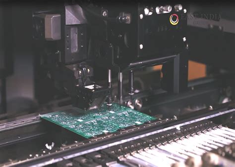
SMT Assembly Process
The SMT assembly process involves several steps to place and solder components onto the PCB:
-
Solder paste printing: A stainless steel stencil is placed over the PCB, and solder paste is deposited onto the component pads through openings in the stencil. The paste is a mixture of tiny solder spheres and flux, which helps clean the metal surfaces and prevent oxidation during soldering.
-
Component placement: The PCB is loaded into a pick-and-place machine, which uses computer vision and precision nozzles to pick up SMT components from feeders and place them onto the solder paste deposits on the board. High-speed machines can place tens of thousands of components per hour with high accuracy.
-
Reflow soldering: After placement, the PCB is conveyed through a reflow oven, which heats the board in a controlled profile to melt the solder paste and form permanent solder joints between the component leads and pads. The oven temperature typically ramps up to a peak of 220-250°C and then cools down gradually to solidify the joints.
-
Inspection and testing: The assembLED PCB undergoes automated optical inspection (AOI) to check for missing or misaligned components, solder defects, or other visible issues. Electrical testing, such as in-circuit test (ICT) or functional test, is also performed to ensure that the board operates correctly before proceeding to final assembly or integration into a product.

Challenges and Considerations
While SMT offers many benefits, it also presents some challenges and requires careful consideration in PCB design and assembly:
-
Component selection: Designers must choose SMT components that are compatible with the assembly process and meet the performance, reliability, and cost requirements of the application. Some components may not be available in SMT packages, or may require special handling or processing.
-
PCB layout: SMT components have specific land pattern and spacing requirements that must be adhered to in the PCB design. The layout must also consider the placement and routing of components to minimize the risk of assembly defects, such as bridging or tombstoning, and to ensure good manufacturability and testability.
-
Thermal management: SMT components can generate significant heat, especially in high-power or high-speed applications. The PCB layout and assembly process must provide adequate thermal dissipation to prevent overheating and ensure long-term reliability. This may involve the use of thermal pads, heat sinks, or other cooling techniques.
-
Rework and repair: SMT boards can be more difficult to rework or repair than through-hole boards, due to the small size and close spacing of components. Special tools and techniques, such as hot-air rework stations and microscopes, may be needed to remove and replace defective components without damaging the board or neighboring parts.

Frequently Asked Questions (FAQ)
What is the difference between surface-mount technology (SMT) and through-hole technology (THT)?
SMT components are mounted directly onto the surface of the PCB, while THT components have leads that are inserted through holes in the board and soldered on the opposite side. SMT allows for smaller components, higher density, and faster assembly compared to THT.
Can SMT and THT components be used on the same PCB?
Yes, PCBs can be designed with a mix of SMT and THT components, known as a hybrid assembly. This is often done to accommodate through-hole connectors, large power components, or other parts that are not available in SMT packages. However, the assembly process is more complex and may require additional steps or equipment.
What is the smallest size of SMT component?
The smallest common SMT chip size is 0201, which measures 0.02″ by 0.01″ (0.5 mm by 0.25 mm). Even smaller sizes, such as 01005 (0.4 mm by 0.2 mm) and 0075 (0.3 mm by 0.15 mm), are used in some high-density applications, but they require specialized handling and assembly equipment.
How do you solder SMT components by hand?
Manual soldering of SMT components can be done using a fine-tip soldering iron, tweezers, and solder wire. The basic steps are:
1. Apply a small amount of solder paste or flux to the component pads on the PCB.
2. Use tweezers to place the component onto the pads, aligning it carefully.
3. Touch the tip of the soldering iron to the component lead and pad, and apply a small amount of solder wire to form a joint. Repeat for each lead.
4. Clean any excess flux or solder with isopropyl alcohol and inspect the joints for good wetting and shape.
Hand soldering of SMT components requires steady hands, good eyesight, and practice to achieve reliable results. It is best suited for prototyping, repair, or low-volume assembly.
What is the expected lifespan of SMT solder joints?
The lifespan of SMT solder joints depends on various factors, including the component type, package size, PCB material, solder alloy, and operating environment. Under typical consumer electronics conditions, a well-designed and assembled SMT joint can last for decades or the entire product life cycle.
However, solder joints can degrade over time due to thermal cycling, mechanical stress, or chemical corrosion. In high-reliability applications, such as aerospace or medical devices, additional measures may be taken to ensure the long-term integrity of SMT joints, such as conformal coating, underfill, or the use of special solder alloys.
Conclusion
Surface-mount technology has revolutionized the electronics industry by enabling smaller, faster, and more cost-effective product designs. Its benefits have made it the dominant method of circuit board assembly for most applications.
However, SMT also presents challenges in component selection, PCB layout, thermal management, and rework that require careful consideration and expertise. As electronic devices continue to advance in complexity and miniaturization, SMT will evolve with new materials, processes, and tools to meet the ever-increasing demands of the industry.
By understanding the fundamentals of SMT, including its advantages, component packages, assembly process, and design considerations, engineers and technicians can effectively utilize this technology to create innovative, reliable, and high-performance electronic products.


Leave a Reply