What are Printed Circuit Boards?
Printed Circuit Boards (PCBs) are the backbone of modern electronics. They are flat boards made of insulating material, such as fiberglass or composite epoxy, with conductive pathways etched or printed onto the surface. These pathways, known as traces, connect various electronic components, such as resistors, capacitors, and integrated circuits, to form a complete electronic circuit.
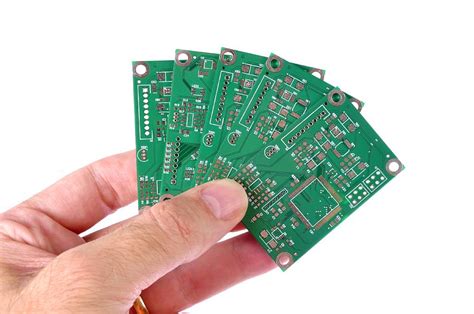
PCBs come in various sizes, shapes, and complexity levels, depending on the application they are designed for. They can range from simple single-layer boards for basic electronic devices to complex multi-layer boards used in advanced computing systems and telecommunications equipment.
Types of Printed Circuit Boards
There are several types of PCBs, each with its own unique characteristics and manufacturing process:
-
Single-Sided PCBs: These boards have conductive traces on only one side of the insulating substrate. They are the simplest and most cost-effective type of PCB, suitable for low-complexity circuits.
-
Double-sided PCBs: These boards have conductive traces on both sides of the insulating substrate, allowing for more complex circuits and higher component density. The two sides are connected using through-hole technology or vias.
-
Multi-layer PCBs: These boards consist of multiple layers of insulating material with conductive traces on each layer. The layers are bonded together using heat and pressure, and the traces are connected using vias. Multi-layer PCBs enable highly complex circuits with high component density, making them ideal for advanced electronics applications.
-
Flexible PCBs: These boards are made of flexible insulating material, such as polyimide, allowing them to bend and conform to various shapes. They are often used in applications where space is limited or where the board needs to flex during operation, such as in wearable devices or automotive electronics.
-
Rigid-flex PCBs: These boards combine the benefits of rigid and flexible PCBs, consisting of both rigid and flexible sections. The rigid sections provide structural support and house most of the components, while the flexible sections allow for connectivity between the rigid sections or to other parts of the device.
Factors Affecting the Mass of Printed Circuit Boards
The mass of a PCB depends on several factors, including the board’s size, thickness, material composition, and the number and type of components mounted on it.
Board Size and Thickness
The size and thickness of a PCB directly impact its mass. Larger boards with more surface area will naturally weigh more than smaller boards. Similarly, thicker boards will have a higher mass than thinner ones, as they contain more insulating material.
PCB Thickness is typically measured in mils (thousandths of an inch) or millimeters. Common PCB thicknesses range from 0.4 mm to 3.2 mm, with 1.6 mm being a standard thickness for many applications.
| PCB Thickness (mm) | PCB Thickness (mils) | Typical Application |
|---|---|---|
| 0.4 | 15.7 | Flexible PCBs |
| 0.8 | 31.5 | High-density PCBs |
| 1.6 | 63.0 | Standard PCBs |
| 2.4 | 94.5 | Heavy-duty PCBs |
| 3.2 | 126.0 | Extreme-duty PCBs |
Material Composition
The material composition of a PCB also plays a significant role in determining its mass. The most common insulating materials used in PCBs are:
-
FR-4: A composite material made of woven fiberglass cloth with an epoxy resin binder. It is the most widely used PCB material due to its excellent mechanical, thermal, and electrical properties.
-
CEM-1: A composite material made of a mixture of woven fiberglass cloth and cellulose paper with an epoxy resin binder. It is a lower-cost alternative to FR-4, with slightly inferior properties.
-
Polyimide: A high-performance polymer material used in flexible and rigid-flex PCBs. It offers excellent thermal stability, chemical resistance, and mechanical strength.
The conductive traces on a PCB are typically made of copper, which is an excellent electrical conductor and relatively inexpensive. The thickness of the copper layer is expressed in ounces per square foot (oz/ft²) or micrometers (µm). Common copper thicknesses range from 0.5 oz/ft² (17.5 µm) to 2 oz/ft² (70 µm), with 1 oz/ft² (35 µm) being the most common.
| Copper Thickness (oz/ft²) | Copper Thickness (µm) | Typical Application |
|---|---|---|
| 0.5 | 17.5 | Low-current PCBs |
| 1.0 | 35.0 | Standard PCBs |
| 2.0 | 70.0 | High-current PCBs |
Number and Type of Components
The number and type of components mounted on a PCB also contribute to its overall mass. More components generally lead to a higher mass, as each component adds its own weight to the board.
The type of components used can also affect the PCB’s mass. Some common component types and their typical masses are:
| Component Type | Typical Mass Range |
|---|---|
| Surface Mount Resistors | 1 – 10 mg |
| Surface Mount Capacitors | 1 – 100 mg |
| Surface Mount Inductors | 10 – 500 mg |
| Surface Mount ICs | 10 – 1000 mg |
| Through-hole Resistors | 100 – 1000 mg |
| Through-hole Capacitors | 100 – 5000 mg |
| Through-hole Inductors | 500 – 10000 mg |
| Through-hole Connectors | 1000 – 50000 mg |

Calculating the Mass of a Printed Circuit Board
To estimate the mass of a PCB, you can use the following formula:
PCB Mass = (Board Area × Board Thickness × Board Density) + (Number of Components × Average Component Mass)
Here’s a step-by-step guide to calculating the mass of a PCB:
- Determine the board area in square centimeters (cm²).
- Measure the board thickness in centimeters (cm).
- Look up the density of the board material in grams per cubic centimeter (g/cm³).
- FR-4: 1.85 g/cm³
- CEM-1: 1.70 g/cm³
- Polyimide: 1.42 g/cm³
- Multiply the board area, thickness, and density to obtain the mass of the Bare Board.
- Count the number of components on the board.
- Estimate the average mass of the components based on their type and size.
- Multiply the number of components by the average component mass to obtain the total component mass.
- Add the bare board mass and the total component mass to get the estimated PCB mass.
Example Calculation
Let’s calculate the mass of a 10 cm × 15 cm double-sided FR-4 PCB with a thickness of 1.6 mm (0.16 cm) and 200 surface mount components with an average mass of 50 mg each.
- Board Area = 10 cm × 15 cm = 150 cm²
- Board Thickness = 0.16 cm
- Board Density (FR-4) = 1.85 g/cm³
- Bare Board Mass = 150 cm² × 0.16 cm × 1.85 g/cm³ = 44.4 g
- Number of Components = 200
- Average Component Mass = 50 mg = 0.05 g
- Total Component Mass = 200 × 0.05 g = 10 g
- Estimated PCB Mass = 44.4 g + 10 g = 54.4 g

Impact of PCB Mass on Electronic Device Design
The mass of a PCB can have significant implications for the design and performance of electronic devices. Some key considerations include:
Weight and Portability
In portable devices, such as smartphones, tablets, and laptops, the mass of the PCB directly affects the overall weight of the device. Designers often strive to minimize PCB mass to improve device portability and user experience. This can be achieved through the use of smaller, thinner boards, advanced materials, and high-density component packaging.
Mechanical Stress and Vibration
The mass of a PCB can also affect its mechanical performance, particularly in applications subject to high stress or vibration. Heavier boards may be more susceptible to mechanical failure due to increased inertial forces. In such cases, designers may need to reinforce the board structure, use vibration-dampening materials, or optimize component placement to minimize mechanical stress.
Thermal Management
The mass of a PCB can impact its thermal performance, as heavier boards may have a higher thermal capacity and take longer to dissipate heat. This can be particularly important in high-power applications or devices with tight thermal constraints. Designers may need to incorporate additional thermal management solutions, such as heatsinks or cooling fans, to ensure proper heat dissipation.
Manufacturing and Assembly
PCB mass can also have implications for manufacturing and assembly processes. Heavier boards may require more robust handling equipment and may be more susceptible to damage during transportation. In addition, the placement of heavy components on a PCB can affect the board’s balance and require specialized assembly techniques to ensure proper alignment and soldering.

Frequently Asked Questions (FAQ)
- What is the most common PCB material, and how does it affect the board’s mass?
-
The most common PCB material is FR-4, a composite of woven fiberglass cloth and epoxy resin. FR-4 has a density of 1.85 g/cm³, which directly contributes to the board’s mass. Using alternative materials with lower densities, such as polyimide (1.42 g/cm³), can help reduce the overall mass of the PCB.
-
How does the number of layers in a PCB affect its mass?
-
As the number of layers in a PCB increases, so does its mass. Each additional layer adds more insulating material and copper traces to the board, increasing its overall thickness and weight. However, using multi-layer PCBs can also help reduce the board’s surface area, as the increased routing density allows for more compact designs.
-
What is the typical mass range for a smartphone PCB?
-
The mass of a smartphone PCB can vary depending on the device’s size and complexity. A typical smartphone PCB may weigh between 10 to 30 grams, with smaller devices on the lower end of the range and larger, more feature-rich devices on the higher end. This mass accounts for both the bare board and the mounted components.
-
How can designers minimize the mass of a PCB without compromising performance?
-
Designers can employ several strategies to minimize PCB mass, such as:
- Using thinner, lighter board materials
- Reducing the board’s surface area through compact, high-density layouts
- Utilizing smaller, lighter components, such as chip-scale packages or bare die
- Optimizing the number of layers to balance routing density and board thickness
- Incorporating advanced manufacturing techniques, such as HDI (High-Density Interconnect) or embedded components
-
What role does PCB mass play in aerospace and aviation electronics?
- In aerospace and aviation applications, minimizing PCB mass is crucial for reducing overall system weight and improving fuel efficiency. Designers often use advanced materials, such as high-performance polymers or ceramic substrates, to create lightweight, yet robust PCBs. They also prioritize high-density, multi-layer designs to minimize board size and weight. Additionally, aerospace PCBs must be designed to withstand harsh environmental conditions, such as extreme temperatures, vibrations, and radiation, which can further influence material selection and board mass.


Leave a Reply