Introduction to Flexible PCB
Flexible printed circuit boards (PCBs) have revolutionized the electronics industry by providing a versatile and compact solution for interconnecting electronic components in various devices. Unlike traditional rigid PCBs, flexible PCBs are made from thin, pliable materials that can bend, fold, and twist without compromising their electrical functionality. This unique characteristic has made flexible PCBs an essential component in the design and manufacturing of compact, lightweight, and portable electronic devices.
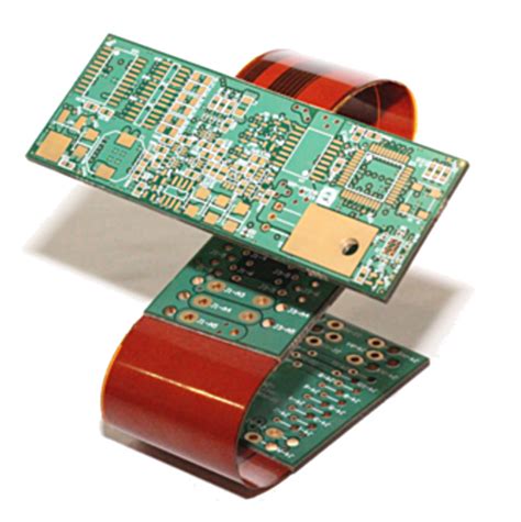
What is a Flexible PCB?
A flexible PCB, also known as a flex circuit or flexboard, is a type of printed circuit board that consists of a thin, flexible substrate with conductive traces and components mounted on its surface. The substrate is typically made from materials such as polyimide, polyester, or other flexible polymers, while the conductive traces are usually made from copper.
Advantages of Flexible PCBs
Flexible PCBs offer several advantages over traditional rigid PCBs, including:
- Compact design: Flexible PCBs can be bent, folded, and shaped to fit into tight spaces, allowing for more compact and lightweight electronic devices.
- Reduced weight: The thin, lightweight materials used in flexible PCBs contribute to an overall reduction in the weight of electronic devices.
- Improved reliability: Flexible PCBs can withstand vibrations, shocks, and extreme temperatures better than rigid PCBs, ensuring higher reliability in harsh environments.
- Enhanced signal integrity: The shorter interconnects and reduced parasitic capacitance in flexible PCBs lead to improved signal integrity and reduced electromagnetic interference (EMI).
- Cost-effective: Flexible PCBs can simplify the assembly process and reduce the number of connectors required, resulting in cost savings.
Applications of Flexible PCB
Flexible PCBs find applications in a wide range of industries and products, including:
Consumer Electronics
Flexible PCBs are extensively used in consumer electronics, such as:
- Smartphones
- Wearables (smartwatches, fitness trackers)
- Cameras
- Laptops and tablets
- Virtual reality (VR) and augmented reality (AR) devices
The compact and lightweight nature of flexible PCBs enables manufacturers to create slim, portable, and feature-rich consumer electronic devices.
Medical Devices
Flexible PCBs are crucial in the development of advanced medical devices, such as:
- Implantable devices (pacemakers, neurostimulators)
- Wearable health monitors
- Diagnostic equipment
- Surgical instruments
The biocompatibility and flexibility of flexible PCBs make them suitable for use in medical devices that require conformity to the human body and long-term reliability.
Automotive Electronics
Flexible PCBs are increasingly used in automotive electronics, particularly in applications that require compact and reliable solutions, such as:
- Infotainment systems
- Advanced driver assistance systems (ADAS)
- Electronic control units (ECUs)
- Sensors and actuators
The ability of flexible PCBs to withstand harsh environmental conditions, such as extreme temperatures and vibrations, makes them ideal for automotive applications.
Aerospace and Defense
Flexible PCBs are employed in various aerospace and defense applications, including:
- Avionics
- Satellite systems
- Radar and communication equipment
- Military wearables
The lightweight and high-reliability characteristics of flexible PCBs are essential for aerospace and defense applications, where weight reduction and performance are critical factors.

Flexible PCB Design Considerations
Designing flexible PCBs requires careful consideration of several factors to ensure optimal performance and reliability. Some key design considerations include:
Material Selection
Choosing the right substrate material is crucial for the success of a flexible PCB design. The most common substrate materials used in flexible PCBs are:
- Polyimide (PI): Known for its excellent thermal stability, chemical resistance, and mechanical properties.
- Polyester (PET): Offers good electrical properties and is cost-effective, but has lower temperature resistance compared to polyimide.
- Liquid Crystal Polymer (LCP): Provides superior high-frequency performance and low moisture absorption, making it suitable for RF applications.
The choice of substrate material depends on the specific application requirements, such as temperature range, flexibility, and dielectric properties.
Conductor Material and Thickness
Copper is the most widely used conductor material in flexible PCBs due to its excellent electrical conductivity and mechanical properties. The thickness of the copper traces is an important design consideration, as it affects the flexibility, current-carrying capacity, and signal integrity of the circuit.
Typical copper thicknesses used in flexible PCBs range from 18 µm to 70 µm (0.5 oz to 2 oz). Thinner copper traces provide better flexibility but have lower current-carrying capacity, while thicker traces offer higher current-carrying capacity but reduced flexibility.
Bend Radius and Flex Life
The bend radius and flex life are critical design parameters in flexible PCBs. The bend radius refers to the minimum radius at which the PCB can be bent without causing damage to the copper traces or the substrate. The flex life is the number of flex cycles the PCB can withstand before failure.
Designers must consider the bend radius and flex life requirements of the application and select appropriate materials, copper thicknesses, and layout techniques to ensure the reliable operation of the flexible PCB over its intended lifespan.
Adhesive Selection
Adhesives play a crucial role in bonding the copper traces to the substrate and laminating multiple layers of flexible PCBs. The choice of adhesive depends on factors such as the substrate material, operating temperature range, and chemical resistance requirements.
Common adhesives used in flexible PCBs include:
- Acrylic: Offers good adhesion and flexibility but has limited temperature resistance.
- Epoxy: Provides excellent chemical and temperature resistance but has lower flexibility compared to acrylic.
- Pressure-sensitive adhesive (PSA): Allows for easy assembly and disassembly of flexible PCBs but has lower temperature resistance and bonding strength compared to other adhesives.
Layout Techniques
Designing the layout of a flexible PCB requires special considerations to ensure the reliability and performance of the circuit. Some key layout techniques include:
- Strain relief: Incorporating strain relief features, such as curved traces or accordion-like folds, to minimize stress on the copper traces during flexing.
- Teardrops: Adding teardrops at the junction of traces and pads to reduce stress concentration and improve the reliability of the solder joints.
- Staggered traces: Offsetting adjacent traces to reduce the risk of shorting due to compression during flexing.
- Hatched polygons: Using hatched polygons instead of solid copper fills to improve flexibility and reduce the risk of cracking.
Designers should also follow recommended design rules, such as minimum trace width and spacing, to ensure the manufacturability and reliability of the flexible PCB.

Flexible PCB Manufacturing Process
The manufacturing process for flexible PCBs is similar to that of rigid PCBs, with some additional steps to accommodate the unique properties of flexible materials. The main steps in the flexible PCB manufacturing process are:
- Substrate preparation: The flexible substrate material is cut to size and cleaned to remove any contaminants.
- Copper lamination: A thin layer of copper is laminated onto the substrate using heat and pressure.
- Patterning: The desired circuit pattern is transferred onto the copper layer using photolithography or laser direct imaging (LDI).
- Etching: The unwanted copper is removed using a chemical etching process, leaving behind the desired circuit pattern.
- Coverlay application: A protective coverlay is applied over the circuitry to provide insulation and mechanical protection.
- Drilling and cutting: Holes are drilled for component mounting and the PCB is cut to its final shape.
- Surface finishing: A surface finish, such as gold plating or solder mask, is applied to protect the copper traces and improve solderability.
- Assembly: Electronic components are mounted onto the flexible PCB using various assembly techniques, such as surface mount technology (SMT) or chip-on-flex (COF).

Flexible PCB Assembly Techniques
Assembling components onto flexible PCBs requires specialized techniques to ensure reliable and robust connections. Some common assembly techniques used for flexible PCBs include:
Surface Mount Technology (SMT)
SMT is a widely used assembly technique for mounting components onto flexible PCBs. In this process, solder paste is applied to the pads on the PCB, and components are placed onto the pads using pick-and-place machines. The PCB then goes through a reflow oven, where the solder paste melts and forms a strong electrical and mechanical connection between the components and the PCB.
Chip-on-Flex (COF)
COF is an advanced assembly technique that involves directly bonding bare semiconductor chips onto the flexible PCB. This technique eliminates the need for a package substrate, resulting in a more compact and lightweight assembly. COF is commonly used in applications that require high-density interconnects and minimal package size, such as mobile phone cameras and displays.
Anisotropic Conductive Film (ACF) Bonding
ACF bonding is a popular assembly technique for connecting flexible PCBs to displays or other substrates. In this process, an anisotropic conductive film, which contains conductive particles dispersed in an adhesive matrix, is placed between the flexible PCB and the substrate. Heat and pressure are applied to the assembly, causing the conductive particles to form electrical connections between the corresponding pads on the PCB and the substrate.
Soldering
Traditional soldering techniques, such as hand soldering or wave soldering, can also be used for assembling components onto flexible PCBs. However, special care must be taken to avoid damaging the flexible substrate or components during the soldering process. Using low-temperature solder alloys and controlled heating methods can help minimize the risk of damage.
Flexible PCB Testing and Quality Control
Ensuring the quality and reliability of flexible PCBs is essential for their successful application in various electronic devices. Several testing and quality control methods are employed to verify the performance and integrity of flexible PCBs, including:
Continuity and Isolation Testing
Continuity testing is performed to ensure that all the intended electrical connections on the flexible PCB are intact and have low resistance. Isolation testing, on the other hand, verifies that there are no short circuits or unintended connections between different parts of the circuit. These tests are typically conducted using a multimeter or a dedicated continuity tester.
Flexible Endurance Testing
Flexible endurance testing is carried out to evaluate the ability of the flexible PCB to withstand repeated bending and flexing without deterioration in electrical performance or mechanical integrity. This test involves subjecting the PCB to a specified number of flex cycles at a defined bend radius and assessing its performance after each cycle.
Environmental Testing
Environmental testing is performed to assess the ability of the flexible PCB to operate reliably under various environmental conditions, such as extreme temperatures, humidity, and vibration. Some common environmental tests include:
- Thermal cycling: Exposing the PCB to alternating high and low temperatures to simulate thermal stress.
- Humidity testing: Subjecting the PCB to high humidity levels to evaluate its resistance to moisture.
- Vibration and shock testing: Assessing the PCB’s ability to withstand mechanical vibrations and shocks.
Microsectioning and Failure Analysis
Microsectioning is a destructive testing method that involves cross-sectioning the flexible PCB to examine its internal structure and identify any manufacturing defects or assembly issues. This technique is commonly used for failure analysis, where the root cause of a PCB failure is investigated by analyzing the cross-sectioned sample under a microscope.
Automated Optical Inspection (AOI)
AOI is a non-destructive testing method that uses high-resolution cameras and advanced image processing algorithms to detect surface defects, such as solder bridges, missing components, or misaligned parts, on the assembled flexible PCB. AOI systems can quickly scan the entire PCB and identify potential issues, enabling early detection and correction of defects.
Future Trends in Flexible PCB Technology
As the demand for compact, lightweight, and flexible electronic devices continues to grow, flexible PCB technology is expected to evolve and advance further. Some of the future trends in flexible PCB technology include:
Increased Adoption of High-Frequency Materials
With the growing demand for high-speed data transmission and wireless connectivity, there is a rising need for flexible PCBs that can support high-frequency signals. Materials such as liquid crystal polymer (LCP) and polytetrafluoroethylene (PTFE) are expected to gain more prominence in flexible PCB design due to their excellent high-frequency performance and low dielectric loss.
Integration of Printed Electronics
Printed electronics, which involve the use of conductive inks and additive manufacturing techniques to create electronic circuits, are expected to be increasingly integrated with flexible PCBs. This integration will enable the creation of novel, low-cost, and environmentally friendly electronic devices with unique form factors and functionalities.
Advancements in Stretchable Electronics
Stretchable electronics, which can conform to complex three-dimensional shapes and withstand significant mechanical deformation, are an emerging area of research in flexible PCB technology. The development of new materials, such as stretchable conductive inks and elastomeric substrates, is expected to drive the growth of stretchable electronics and enable new applications in wearable devices, soft robotics, and biomedical implants.
Increased Use of Embedded Components
Embedding electronic components, such as resistors, capacitors, and integrated circuits, directly into the flexible PCB substrate is a growing trend in flexible PCB design. This approach offers several benefits, including reduced assembly complexity, improved signal integrity, and enhanced mechanical reliability. As the demand for more compact and integrated electronic devices continues to rise, the use of embedded components in flexible PCBs is expected to become more widespread.
Frequently Asked Questions (FAQ)
1. What is the difference between a flexible PCB and a rigid PCB?
A flexible PCB is made from thin, pliable materials that can bend, fold, and twist without compromising its electrical functionality, while a rigid PCB is made from a solid, inflexible substrate material, such as FR-4. Flexible PCBs offer several advantages over rigid PCBs, including compact design, reduced weight, improved reliability, and enhanced signal integrity.
2. What are the most common substrate materials used in flexible PCBs?
The most common substrate materials used in flexible PCBs are polyimide (PI), polyester (PET), and liquid crystal polymer (LCP). Polyimide is known for its excellent thermal stability, chemical resistance, and mechanical properties, while polyester offers good electrical properties and is cost-effective. Liquid crystal polymer provides superior high-frequency performance and low moisture absorption, making it suitable for RF applications.
3. What is the typical copper thickness used in flexible PCBs?
Typical copper thicknesses used in flexible PCBs range from 18 µm to 70 µm (0.5 oz to 2 oz). Thinner copper traces provide better flexibility but have lower current-carrying capacity, while thicker traces offer higher current-carrying capacity but reduced flexibility. The choice of copper thickness depends on the specific application requirements, such as current-carrying capacity, flexibility, and signal integrity.
4. What are some common assembly techniques used for flexible PCBs?
Some common assembly techniques used for flexible PCBs include surface mount technology (SMT), chip-on-flex (COF), anisotropic conductive film (ACF) bonding, and soldering. SMT involves mounting components onto the flexible PCB using solder paste and reflow soldering, while COF involves directly bonding bare semiconductor chips onto the flexible PCB. ACF bonding is used for connecting flexible PCBs to displays or other substrates, and traditional soldering techniques can also be used with special care to avoid damaging the flexible substrate or components.
5. What are some future trends in flexible PCB technology?
Some future trends in flexible PCB technology include increased adoption of high-frequency materials, integration of printed electronics, advancements in stretchable electronics, and increased use of embedded components. These trends are driven by the growing demand for compact, lightweight, and flexible electronic devices with advanced functionalities and high-speed connectivity.
| Substrate Material | Characteristics | Typical Applications |
|---|---|---|
| Polyimide (PI) | Excellent thermal stability, chemical resistance, and mechanical properties | High-reliability electronics, aerospace, and defense |
| Polyester (PET) | Good electrical properties, cost-effective | Consumer electronics, medical devices |
| Liquid Crystal Polymer (LCP) | Superior high-frequency performance, low moisture absorption | RF and high-speed electronics, automotive |
| Assembly Technique | Description | Advantages |
|---|---|---|
| Surface Mount Technology (SMT) | Components mounted onto PCB using solder paste and reflow soldering | Widely used, suitable for various component types |
| Chip-on-Flex (COF) | Bare semiconductor chips directly bonded onto flexible PCB | Compact and lightweight assembly, high-density interconnects |
| Anisotropic Conductive Film (ACF) Bonding | Conductive film used to connect flexible PCB to displays or substrates | Enables reliable connections between flexible PCBs and other substrates |
| Soldering | Traditional soldering techniques used with special care for flexible PCBs | Widely used, suitable for various component types |
In conclusion, flexible PCBs have revolutionized the electronics industry by providing a versatile and compact solution for interconnecting electronic components in various devices. Their unique ability to bend, fold, and twist without compromising electrical functionality has made them an essential component in the design and manufacturing of compact


Leave a Reply