The Basics of Through-hole PCB Assembly
Understanding Through-hole Technology
Through-hole technology involves mounting components on a PCB by inserting their leads through drilled holes. The leads are then soldered to pads on the opposite side of the board, creating a strong mechanical and electrical connection. This assembly method is known for its durability and reliability, making it suitable for applications that require high levels of mechanical stress or exposure to harsh environments.
Components Used in Through-hole PCB Assembly
Through-hole components come in various shapes and sizes, each designed for specific functions. Some common through-hole components include:
- Resistors
- Capacitors
- Inductors
- Diodes
- Transistors
- Integrated circuits (ICs)
- Connectors
- Switches
These components are typically larger than their surface-mount counterparts, making them easier to handle and replace when necessary.
Advantages of Through-hole PCB Assembly
Mechanical Strength
One of the primary advantages of through-hole PCB assembly is its superior mechanical strength. The leads of through-hole components are inserted through the board and soldered on the opposite side, creating a strong physical connection. This makes the assembly more resistant to vibration, shock, and other mechanical stresses, ensuring a longer lifespan for the PCB.
Ease of Manual Assembly
Through-hole components are generally larger and easier to handle than surface-mount components, making manual assembly more straightforward. This is particularly beneficial for low-volume production runs, prototyping, or hobbyist projects where automated assembly may not be cost-effective or necessary.
Simplified Inspection and Repair
The larger size of through-hole components and the visibility of the solder joints make it easier to inspect the assembled PCB for defects or errors. If a component needs to be replaced, it can be easily desoldered and removed without damaging the board or surrounding components.
Compatibility with High-power Applications
Through-hole components often have higher power ratings compared to surface-mount components, making them suitable for applications that require high currents or voltages. The larger lead diameter and the ability to dissipate heat through the board contribute to the increased power handling capacity of through-hole components.

Disadvantages of Through-hole PCB Assembly
Lower Component Density
Through-hole components require drilled holes and larger pad sizes, which occupy more space on the PCB compared to surface-mount components. This limits the component density and can result in larger board sizes, especially for complex designs with numerous components.
Increased Manufacturing Time and Cost
The process of drilling holes and manually inserting components during through-hole PCB assembly is more time-consuming compared to automated surface-mount assembly. This can lead to higher manufacturing costs, particularly for high-volume production runs.
Limited Design Flexibility
The need for drilled holes and the larger size of through-hole components can restrict design flexibility, making it challenging to create compact or intricate PCB layouts. This limitation can be a drawback for applications that require miniaturization or advanced functionality.

The Through-hole PCB Assembly Process
PCB Design and Fabrication
The through-hole PCB assembly process begins with the design and fabrication of the printed circuit board. The PCB design includes the component layout, trace routing, and the placement of drilled holes for through-hole components. Once the design is finalized, the PCB is fabricated using a multi-step process that involves applying copper layers, etching circuits, laminating, drilling holes, and applying a protective solder mask and silkscreen.
Component Insertion
After the PCB is fabricated, the through-hole components are inserted into the drilled holes. This process can be done manually or using automated insertion machines, depending on the production volume and available resources. Manual insertion is common for low-volume runs or prototypes, while automated insertion is more efficient for high-volume production.
Soldering
Once the components are inserted, the PCB undergoes a soldering process to create a permanent electrical and mechanical connection between the component leads and the PCB pads. There are two primary methods for soldering through-hole components:
-
Wave Soldering: The PCB is passed over a molten solder wave, which flows into the holes and creates a solder joint on the opposite side of the board.
-
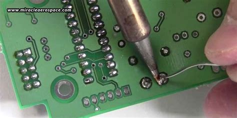
Hand Soldering: For low-volume production or prototypes, soldering can be done manually using a soldering iron and solder wire.
Inspection and Testing
After soldering, the assembled PCB undergoes inspection and testing to ensure the quality and functionality of the board. Visual inspection is performed to check for any soldering defects, such as bridging, cold joints, or insufficient solder. Electrical testing is conducted to verify the continuity and performance of the PCB, ensuring that it meets the specified requirements.
Cleaning and Finishing
The final step in the through-hole PCB assembly process is cleaning and finishing. Any flux residue or contaminants are removed from the board using solvents or cleaning agents. If required, additional finishing processes, such as conformal coating or potting, may be applied to protect the PCB from environmental factors or to enhance its mechanical strength.

Applications of Through-hole PCB Assembly
Through-hole PCB assembly finds applications in various industries and sectors, including:
- Aerospace and Defense
- Automotive Electronics
- Industrial Control Systems
- Medical Devices
- Power Electronics
- Consumer Electronics (e.g., audio equipment, appliances)
- Hobbyist and DIY Projects
The choice between through-hole and surface-mount assembly depends on factors such as the specific application requirements, production volume, cost constraints, and the level of mechanical stress or environmental exposure the PCB will encounter.
Comparing Through-hole and Surface-mount PCB Assembly
| Characteristic | Through-hole PCB Assembly | Surface-mount PCB Assembly |
|---|---|---|
| Component Size | Larger | Smaller |
| Component Density | Lower | Higher |
| Mechanical Strength | Higher | Lower |
| Assembly Process | Manual or Automated Insertion, Wave or Hand Soldering | Automated Pick-and-Place, Reflow Soldering |
| Manufacturing Cost | Higher for High-volume Production | Lower for High-volume Production |
| Design Flexibility | Limited | Higher |
| Rework and Repair | Easier | More Challenging |
While surface-mount technology has gained prominence in recent years due to its advantages in component density, manufacturing efficiency, and cost-effectiveness for high-volume production, through-hole PCB assembly remains a reliable and preferred choice for certain applications and scenarios.
Frequently Asked Questions (FAQ)
-
Q: What is the difference between through-hole and surface-mount PCB assembly?
A: Through-hole PCB assembly involves inserting component leads through drilled holes in the board and soldering them on the opposite side, while surface-mount assembly places components directly on the surface of the PCB and solders them in place. -
Q: When should I choose through-hole PCB assembly over surface-mount?
A: Through-hole PCB assembly is preferred when mechanical strength, ease of manual assembly, or compatibility with high-power components are prioritized. It is also suitable for low-volume production, prototyping, or applications exposed to harsh environments. -
Q: Can through-hole and surface-mount components be used together on the same PCB?
A: Yes, it is possible to design a PCB that incorporates both through-hole and surface-mount components. This is called a mixed-technology or hybrid assembly, and it combines the benefits of both assembly methods. -
Q: Is through-hole PCB assembly more expensive than surface-mount?
A: For high-volume production, through-hole PCB assembly is generally more expensive due to the increased manufacturing time and the cost of drilling holes. However, for low-volume production or prototypes, through-hole assembly can be more cost-effective. -
Q: Are through-hole components becoming obsolete?
A: While surface-mount technology has become increasingly popular, through-hole components are still widely used and continue to be manufactured. They remain relevant for specific applications and are not likely to become obsolete in the near future.
In conclusion, through-hole PCB assembly is a well-established and reliable method for manufacturing printed circuit boards. Despite the growing popularity of surface-mount technology, through-hole assembly maintains its relevance in various industries and applications, offering advantages such as mechanical strength, ease of manual assembly, and compatibility with high-power components. By understanding the characteristics, benefits, and limitations of through-hole PCB assembly, designers and manufacturers can make informed decisions when selecting the most suitable assembly method for their specific projects.


Leave a Reply