What is PCB Etching?
PCB etching is the process of removing unwanted copper from a printed circuit board (PCB) to create the desired circuit pattern. It involves applying a resist layer to the copper surface, exposing it to light through a mask or stencil, and then using an etchant solution to dissolve the unprotected copper areas. PCB etching is a crucial step in the fabrication of Custom PCBs for various electronic projects.
Why Etch Your Own PCBs?
There are several reasons why you might want to etch your own PCBs:
- Cost-effective for small-scale projects
- Faster turnaround time compared to outsourcing
- Allows for custom designs and modifications
- Provides a learning opportunity for understanding PCB Fabrication
Materials and Tools Required
Before starting the PCB etching process, gather the following materials and tools:
| Material/Tool | Description |
|---|---|
| Copper-clad board | A substrate with a thin layer of copper on one or both sides |
| Etchant solution | A chemical solution that dissolves copper, such as ferric chloride or ammonium persulfate |
| Resist pen or transfer paper | Used to draw or transfer the circuit pattern onto the copper surface |
| Etching tank or container | A plastic or glass container to hold the etchant solution and the PCB during etching |
| Protective gloves and eyewear | To ensure safety when handling chemicals |
| Drill or drill press | For drilling holes in the PCB for component leads |
| Soldering iron and solder | For attaching components to the etched PCB |
Choosing the Right Copper-Clad Board
Copper-clad boards come in various sizes, thicknesses, and materials. The most common types are:
- FR-4: A fiberglass-reinforced epoxy laminate, widely used for its durability and heat resistance
- Phenolic: A paper-based laminate, less expensive but more brittle than FR-4
- Polyimide: A high-temperature resistant material, suitable for aerospace and military applications
Select the appropriate copper-clad board based on your project requirements and budget.

Designing the Circuit
Creating the Circuit Schematic
Before etching the PCB, you need to design the circuit schematic using electronic design automation (EDA) software or by hand. The schematic should include all the components and their interconnections. Some popular EDA software options are:
- KiCad
- Eagle
- Altium Designer
- OrCAD
Converting Schematic to PCB Layout
Once the schematic is complete, convert it into a PCB layout. This involves arranging the components and routing the traces on the copper-clad board. Consider the following factors when designing the PCB layout:
- Component placement for optimal performance and ease of assembly
- Trace width and spacing to ensure proper current carrying capacity and signal integrity
- Ground planes and power planes for improved signal quality and EMI reduction
- Mounting holes and edge clearances for mechanical stability

Transferring the Circuit Pattern
Using a Resist Pen
A resist pen is a simple and inexpensive way to transfer the circuit pattern onto the copper-clad board. Follow these steps:
- Clean the copper surface with steel wool or fine sandpaper to remove any oxidation
- Print the PCB layout on paper and place it under the copper-clad board
- Trace the pattern using the resist pen, applying even pressure to ensure a consistent line width
- Allow the resist ink to dry completely before proceeding to etching
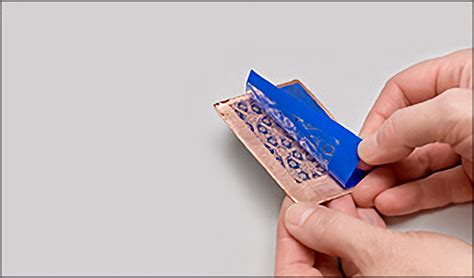
Using Transfer Paper
Transfer paper is a special type of paper coated with a film that can be transferred onto the copper surface using heat. To use transfer paper:
- Print the PCB layout onto the transfer paper using a laser printer
- Cut out the printed pattern, leaving a small margin around the edges
- Clean the copper surface as described earlier
- Place the transfer paper face-down on the copper surface and apply heat using an iron
- Peel off the transfer paper carefully, leaving the toner on the copper surface

Etching the PCB
Preparing the Etchant Solution
The most common etchant solutions used for PCB etching are ferric chloride and ammonium persulfate. Follow the manufacturer’s instructions for preparing the solution and always wear protective gloves and eyewear when handling chemicals.
Etching Process
- Place the PCB in the etching tank or container filled with the etchant solution
- Agitate the solution gently to ensure even etching and prevent bubble formation
- Monitor the etching progress closely, as over-etching can cause the traces to become too thin or disappear entirely
- Remove the PCB from the solution once the unwanted copper has been completely removed
- Rinse the PCB thoroughly with water to stop the etching process
Removing the Resist
After etching, remove the resist layer from the PCB using a suitable solvent, such as acetone or isopropyl alcohol. Gently scrub the surface with a soft brush to ensure complete removal of the resist.
Drilling and Soldering
Drilling Component Holes
Using a drill or drill press, carefully drill holes in the PCB for component leads. Ensure that the hole sizes match the component lead diameters and are positioned accurately according to the PCB layout.
Soldering Components
- Insert the component leads through the drilled holes from the non-copper side of the PCB
- Solder the leads to the copper pads using a soldering iron and solder
- Trim any excess lead length using wire cutters
- Inspect the solder joints for proper connection and remove any solder bridges or splashes
Testing and Troubleshooting
Visual Inspection
Perform a thorough visual inspection of the etched and assembLED PCB. Look for any missing or damaged traces, solder bridges, or cold solder joints. Use a magnifying glass or microscope for detailed inspection.
Continuity Testing
Use a multimeter to test the continuity of the traces and connections. Check for any open circuits or short circuits between adjacent traces. Repair any defects found during testing.
Functional Testing
Power up the assembled PCB and test its functionality according to the circuit design. Use oscilloscopes, logic analyzers, or other diagnostic tools to verify the circuit’s performance and identify any issues.
Frequently Asked Questions (FAQ)
-
Q: Can I reuse the etchant solution?
A: Yes, you can reuse the etchant solution multiple times until it becomes exhausted. The etching process will slow down as the solution weakens, and you may need to replace it when it no longer effectively removes copper. -
Q: How do I dispose of the used etchant solution?
A: Etchant solutions contain harmful chemicals and should be disposed of properly. Contact your local waste management authority for guidance on safe disposal methods. Do not pour the solution down the drain or into the environment. -
Q: Can I use a regular printer to print the PCB layout on transfer paper?
A: No, you should use a laser printer to print the PCB layout on transfer paper. Inkjet printers use water-based inks that will not transfer properly onto the copper surface. -
Q: What should I do if the resist pen or transfer paper does not adhere well to the copper surface?
A: Ensure that the copper surface is clean and free from oxidation. You can use a fine abrasive pad or sandpaper to gently roughen the surface, which can improve the adhesion of the resist or transfer film. -
Q: How can I create double-sided PCBs using the etching method?
A: To create double-sided PCBs, you’ll need to align and register the two sides of the PCB layout accurately. Use registration marks or holes to ensure proper alignment. Etch and drill each side separately, then use through-hole plating or conductive vias to connect the layers.
Conclusion
PCB etching is a valuable skill for anyone interested in electronics and custom PCB fabrication. By following the steps outlined in this article, you can create your own etched PCBs for various projects. Remember to prioritize safety when handling chemicals and always dispose of etchant solutions responsibly.
With practice and experience, you’ll be able to refine your PCB etching techniques and produce high-quality, custom-designed circuit boards for your electronic projects.


Leave a Reply