What is PCB Soldermask and Why is it Important?
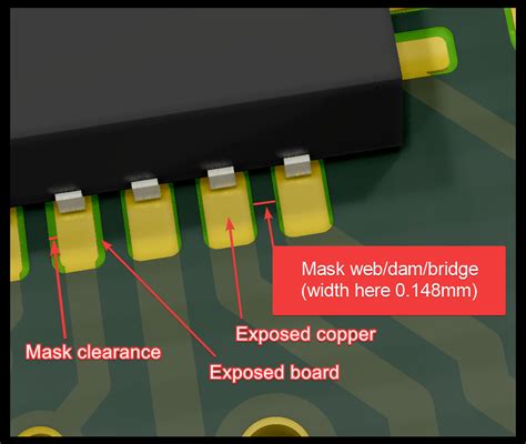
PCB soldermask, also known as solder resist or solder mask, is a thin layer of polymer that is applied to the copper traces of a printed circuit board (PCB). The main purpose of soldermask is to protect the copper traces from oxidation, prevent solder bridges from forming between closely spaced pads, and provide electrical insulation.
Soldermask is crucial for ensuring the reliability and longevity of PCBs. Without proper soldermask coverage, the exposed copper traces can corrode over time due to moisture and other environmental factors. This can lead to electrical shorts, signal integrity issues, and ultimately, PCB failure.
Additionally, soldermask helps to define the areas where solder should be applied during the assembly process. By selectively covering certain areas of the PCB, soldermask ensures that solder only adheres to the exposed pads, preventing unwanted connections between adjacent traces.
Common Problems with PCB Soldermask
Despite its importance, PCB soldermask is not immune to problems. Here are some of the most common issues that can arise:
1. Soldermask Peeling or Lifting
One of the most prevalent problems with PCB soldermask is peeling or lifting. This occurs when the soldermask fails to adhere properly to the copper surface, causing it to separate or lift off the PCB. There are several potential causes of soldermask peeling:
- Contamination: If the copper surface is not thoroughly cleaned prior to applying the soldermask, contaminants such as dirt, grease, or oxidation can prevent proper adhesion.
- Incompatible materials: Using soldermask that is not compatible with the PCB substrate or the copper surface treatment can result in poor adhesion.
- Improper curing: If the soldermask is not cured correctly, either due to insufficient heat or incorrect curing time, it may not fully crosslink and adhere to the copper.
- Mechanical stress: Excessive bending, twisting, or impact can cause the soldermask to crack and peel away from the PCB.
2. Soldermask Cracking
Another common issue is soldermask cracking, which can occur due to various factors:
- Thermal stress: During the soldering process, the PCB is subjected to high temperatures. If the soldermask is not designed to withstand these temperatures, it may crack or become brittle.
- Mechanical stress: As mentioned earlier, excessive bending or twisting of the PCB can cause the soldermask to crack, especially if it is already brittle due to thermal stress.
- Incorrect thickness: If the soldermask is applied too thick or too thin, it may be more prone to cracking under stress.
3. Soldermask Discoloration
Soldermask discoloration is a cosmetic issue that can occur over time due to exposure to UV light, high temperatures, or certain chemicals. While discoloration does not necessarily affect the functionality of the PCB, it can be a concern for applications where appearance is important, such as consumer electronics.
4. Soldermask Residue
During the soldermask application process, excess soldermask may accumulate on the PCB surface, creating a residue that can interfere with the soldering process. If not properly cleaned, this residue can cause issues such as poor solder wetting, weak solder joints, or even prevent components from being soldered at all.
5. Inconsistent Soldermask Coverage
Inconsistent soldermask coverage can occur due to various factors, such as incorrect screen printing parameters, uneven copper surface, or improper cleaning. This can result in areas of the PCB being left exposed or having insufficient Soldermask Thickness, leading to potential reliability issues.

Solutions for PCB Soldermask Problems
Now that we’ve identified some of the most common problems with PCB soldermask, let’s explore potential solutions:
1. Proper Surface Preparation
To prevent soldermask peeling and ensure good adhesion, it is crucial to properly prepare the copper surface prior to applying the soldermask. This involves thoroughly cleaning the PCB to remove any contaminants, such as dirt, grease, or oxidation.
| Cleaning Method | Description |
|---|---|
| Chemical cleaning | Using solvents or detergents to remove organic contaminants |
| Mechanical cleaning | Using abrasive materials, such as sandpaper or brushes, to remove surface oxidation |
| Plasma cleaning | Using ionized gas to remove contaminants and activate the surface for better adhesion |
2. Material Selection
Choosing the right soldermask material is essential for preventing problems such as cracking, peeling, or discoloration. When selecting a soldermask, consider the following factors:
- Compatibility: Ensure that the soldermask is compatible with the PCB substrate material and the copper surface treatment.
- Thermal resistance: Choose a soldermask that can withstand the high temperatures encountered during the soldering process without cracking or becoming brittle.
- Flexibility: For applications where the PCB may be subjected to bending or twisting, select a soldermask with good flexibility to prevent cracking.
- UV resistance: If the PCB will be exposed to UV light, opt for a soldermask with good UV resistance to minimize discoloration over time.
3. Proper Curing
To ensure that the soldermask fully crosslinks and adheres to the copper surface, it is important to follow the manufacturer’s recommended curing process. This typically involves exposing the PCB to a specific temperature for a set duration.
| Curing Method | Description | Typical Temperature Range | Typical Duration |
|---|---|---|---|
| Thermal curing | Exposing the PCB to heat in an oven or on a hotplate | 120-150°C | 30-60 minutes |
| UV curing | Exposing the PCB to UV light to initiate the crosslinking reaction | N/A | 1-5 minutes |
| Combination curing | Using both thermal and UV curing for optimal results | 80-120°C (thermal), N/A (UV) | 10-30 minutes (thermal), 1-5 minutes (UV) |
4. Soldermask Thickness Control
Controlling the soldermask thickness is crucial for preventing issues such as cracking or inconsistent coverage. The optimal thickness depends on the specific application and the soldermask material being used.
| Application | Typical Soldermask Thickness |
|---|---|
| Standard PCBs | 0.8-1.2 mils (20-30 μm) |
| High-density PCBs | 0.4-0.8 mils (10-20 μm) |
| Flexible PCBs | 0.2-0.4 mils (5-10 μm) |
To achieve the desired thickness, use screen printing or curtain coating techniques, and ensure that the process parameters (e.g., mesh size, coating speed) are optimized for the specific soldermask material.
5. Proper Cleaning and Inspection
After applying the soldermask, it is important to clean the PCB thoroughly to remove any residue that may interfere with the soldering process. This can be done using a combination of chemical cleaning agents and mechanical cleaning methods, such as brushing or ultrasonic cleaning.
Once the PCB is clean, perform a visual inspection to check for any defects, such as peeling, cracking, or inconsistent coverage. Automated optical inspection (AOI) systems can be used to quickly and accurately detect soldermask defects, allowing for timely corrections and reducing the risk of PCB failure.

FAQ
1. What is the difference between liquid photoimageable (LPI) and dry film soldermask?
LPI soldermask is applied as a liquid and then exposed to UV light to create the desired pattern, while dry film soldermask is a solid film that is laminated onto the PCB surface and then exposed and developed. LPI soldermask offers better resolution and finer features, while dry film soldermask is more durable and resistant to chemicals.
2. Can soldermask be removed and reapplied if there are defects?
In most cases, soldermask can be removed using a combination of chemical stripping agents and mechanical abrasion. However, removing soldermask can be a time-consuming and delicate process, and it may not always be possible to completely remove all traces of the old soldermask. If soldermask defects are detected early in the manufacturing process, it is often more cost-effective to scrap the affected PCBs and start over.
3. How does soldermask color affect PCB performance?
Soldermask color is primarily a cosmetic choice and does not typically affect PCB performance. However, some colors, such as white or light gray, may be more susceptible to discoloration over time due to UV exposure. Additionally, certain colors may be more difficult to inspect visually, making it harder to detect defects or contamination.
4. Can soldermask be applied selectively to certain areas of the PCB?
Yes, soldermask can be applied selectively using a process called spot masking. This involves applying soldermask only to specific areas of the PCB, such as around component pads or connectors, while leaving other areas exposed. Spot masking can be useful for applications where certain areas of the PCB need to be left exposed for electrical contact or heat dissipation.
5. How can I prevent soldermask from interfering with PCB testing and debugging?
To prevent soldermask from interfering with PCB testing and debugging, consider designing test points or probe pads on the PCB that are left exposed (i.e., not covered by soldermask). These exposed pads allow for easy access to critical signals or components during testing and debugging, without the need to damage or remove the soldermask.

Conclusion
PCB soldermask plays a critical role in protecting the copper traces, preventing solder bridges, and ensuring the overall reliability of the PCB. However, soldermask is not immune to problems, such as peeling, cracking, discoloration, residue, and inconsistent coverage.
To prevent these issues, it is essential to follow best practices for soldermask application, including proper surface preparation, material selection, curing, thickness control, and cleaning. By understanding the common problems and implementing the appropriate solutions, PCB manufacturers can produce high-quality, reliable PCBs that meet the demands of today’s electronics industry.


Leave a Reply