Introduction to Layout-Schematic Relationship
The process of creating a printed circuit board (PCB) involves several crucial steps, and one of the most important is translating the schematic design into a physical layout. The schematic represents the logical connections between components, while the layout determines their physical placement and routing on the PCB. In this article, we will delve into the process of creating a layout from a schematic, exploring best practices, common challenges, and tools that can help streamline the workflow.
Understanding the Schematic
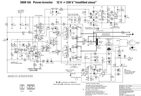
Before diving into the layout process, it is essential to have a solid understanding of the schematic. The schematic is a graphical representation of the electronic circuit, showing the components and their interconnections. It uses standardized symbols to represent various components such as resistors, capacitors, integrated circuits, and connectors.
Here are some key elements of a schematic:
| Element | Description |
|---|---|
| Components | Represented by standardized symbols, such as resistors, capacitors, ICs, etc. |
| Nets | Connections between component pins, represented by lines or wires |
| Labels | Unique identifiers for components, nets, and pins |
| Power and Ground | Symbols representing the power supply and ground connections |
A well-designed schematic should be clear, organized, and easy to follow. It should also include relevant information such as component values, part numbers, and any special requirements.
Importance of a Clean Schematic
Creating a clean and accurate schematic is crucial for a successful layout. A poorly designed schematic can lead to errors, delays, and increased costs during the layout and manufacturing process. Some common issues that can arise from a poorly designed schematic include:
- Incorrect component connections
- Missing or duplicate components
- Inconsistent labeling or naming conventions
- Unclear power and ground connections
To avoid these issues, it is important to follow best practices when creating a schematic, such as:
- Using consistent naming conventions for components, nets, and labels
- Organizing the schematic into logical sections or hierarchies
- Providing clear and concise documentation, including component values and part numbers
- Verifying the schematic against the design requirements and specifications
Preparing for Layout
Before starting the layout process, there are several steps you should take to ensure a smooth and efficient workflow.
Checking the Schematic
The first step is to thoroughly review the schematic for any errors or inconsistencies. This includes:
- Verifying component connections and pinouts
- Checking for missing or duplicate components
- Ensuring consistent labeling and naming conventions
- Confirming power and ground connections
It is also a good idea to have a peer or supervisor review the schematic as a second set of eyes can often catch mistakes that may have been overlooked.
Gathering Component Information
Next, gather all the necessary information about the components used in the design. This includes:
- Physical dimensions (footprint)
- Pin assignments and functions
- Thermal requirements
- Mounting requirements (through-hole, surface-mount, etc.)
This information is typically available in the component datasheets or can be obtained from the manufacturer’s website.
Creating a Component Library
To streamline the layout process, it is helpful to create a library of the components used in the design. This library should include the schematic symbols and the corresponding footprints for each component.
Many PCB design tools, such as Altium Designer, Eagle, and KiCad, include built-in libraries with common components. However, for custom or specialized components, you may need to create your own library.
When creating a component library, consider the following:
- Use consistent naming conventions for components and footprints
- Verify the accuracy of the footprints against the component datasheets
- Include relevant metadata, such as part numbers and manufacturer information
Having a well-organized component library can save significant time and effort during the layout process.
Layout Considerations
When creating a layout from a schematic, there are several key considerations to keep in mind to ensure a successful design.
Board Size and Shape
The first step is to determine the size and shape of the PCB. This will depend on factors such as:
- Enclosure or mounting requirements
- Component placement and routing
- Manufacturing constraints
It is important to consider any physical limitations or constraints early in the design process to avoid issues later on.
Component Placement
Component placement is a critical aspect of PCB layout. Proper placement can improve signal integrity, reduce noise and interference, and minimize the overall board size.
Here are some guidelines for component placement:
- Group related components together to minimize trace lengths and improve signal integrity
- Place sensitive components, such as high-speed ICs or RF circuits, away from noisy components or power supplies
- Consider the thermal requirements of components and provide adequate cooling or heatsinking
- Ensure proper clearance between components for assembly and manufacturing
It is also important to consider the placement of connectors, switches, and other user interface components for ease of use and accessibility.
Routing and Trace Width
Once the components are placed, the next step is to route the connections between them. This involves creating copper traces on the PCB Layers to connect the component pins according to the schematic.
When routing traces, consider the following:
- Use appropriate trace widths based on the current requirements and manufacturing constraints
- Minimize trace lengths to reduce signal loss and interference
- Avoid sharp angles or corners that can cause signal reflections or manufacturing issues
- Provide adequate spacing between traces to prevent crosstalk and signal integrity issues
For high-speed or sensitive signals, it may be necessary to use specialized routing techniques such as differential pairs or controlled impedance traces.
Power and Ground Planes
Proper power and ground distribution is essential for a reliable and stable PCB design. One common technique is to use dedicated power and ground planes on separate layers of the PCB.
Power and ground planes provide a low-impedance path for current flow and help reduce noise and interference. They also provide a reference plane for signal traces, which can improve signal integrity.
When designing power and ground planes, consider the following:
- Use appropriate plane thicknesses based on the current requirements and manufacturing constraints
- Provide adequate Decoupling capacitors near power pins to reduce noise and transient spikes
- Use split planes or isolated regions for sensitive circuits or mixed-signal designs
- Provide proper grounding and shielding for external connections or connectors
Signal Integrity and EMC
Signal integrity and electromagnetic compatibility (EMC) are critical considerations for modern PCB designs, particularly for high-speed or wireless applications.
Signal integrity refers to the ability of a signal to propagate through the PCB without distortion or degradation. Common issues that can affect signal integrity include:
- Reflection and ringing caused by impedance mismatches
- Crosstalk between adjacent traces
- Attenuation and dispersion due to dielectric losses
To mitigate these issues, designers can use techniques such as:
- Impedance matching and termination
- Proper trace routing and spacing
- Use of ground planes and shielding
EMC refers to the ability of a device to operate without causing or being affected by electromagnetic interference (EMI). To ensure EMC compliance, designers should consider:
- Proper grounding and shielding
- Use of filters and suppression components
- Minimizing loop areas and antenna effects
- Compliance with relevant EMC standards and regulations

Layout Tools and Workflow
Creating a PCB layout from a schematic requires specialized tools and a well-defined workflow. Here are some common tools and steps involved in the layout process.
PCB Design Software
There are many PCB design software packages available, ranging from free and open-source tools to high-end commercial solutions. Some popular options include:
- Altium Designer
- Autodesk Eagle
- KiCad
- Cadence Allegro
- Mentor Graphics PADS
When choosing a PCB design tool, consider factors such as ease of use, feature set, integration with other tools, and cost.
Schematic Capture
The first step in the layout process is to capture the schematic in the PCB design software. This involves creating a new project, importing or creating the schematic symbols, and connecting them according to the schematic.
Most PCB design tools include a schematic editor with features such as:
- Symbol libraries and creation tools
- Net and bus management
- Design rule checking (DRC) and electrical rule checking (ERC)
- Cross-probing with the layout editor
Component Placement
Once the schematic is captured, the next step is to place the components on the PCB layout. This involves:
- Importing or creating the component footprints
- Arranging the components according to the placement guidelines
- Ensuring proper orientation and alignment
- Defining the board outline and mounting holes
Many PCB design tools include placement automation features that can help optimize the component placement based on various criteria such as signal flow or thermal requirements.
Routing and Trace Management
After the components are placed, the next step is to route the traces between them according to the schematic connections. This involves:
- Defining the trace widths and spacing based on the design rules
- Routing the traces manually or using autorouting tools
- Adding vias and layer transitions as needed
- Verifying the routing against the design rules and constraints
PCB design tools typically include features such as:
- Interactive and automatic routing modes
- Via and pad stack management
- Trace length and impedance control
- Design rule checking (DRC) and constraint management
Board Stackup and Manufacturing Preparation
Once the routing is complete, the final step is to prepare the design for manufacturing. This involves:
- Defining the board stackup, including layer thicknesses and materials
- Adding manufacturing information such as drill sizes and tolerances
- Generating the manufacturing files, such as Gerber files, drill files, and assembly drawings
- Verifying the design against the manufacturing requirements and constraints
PCB design tools typically include features for stackup management, manufacturing file generation, and design for manufacturing (DFM) analysis.
Best Practices and Tips
Creating a successful PCB layout from a schematic requires a combination of technical skills, attention to detail, and adherence to best practices. Here are some tips and guidelines to keep in mind:
- Start with a clean and well-organized schematic
- Use consistent naming and labeling conventions throughout the design
- Choose appropriate component packages and footprints for the application
- Follow the component manufacturer’s recommendations for placement and routing
- Use appropriate trace widths and spacing based on the current and signal requirements
- Minimize trace lengths and avoid unnecessary layer transitions
- Provide adequate power and ground distribution, including decoupling capacitors
- Consider signal integrity and EMC requirements, particularly for high-speed or sensitive circuits
- Use design rule checking (DRC) and constraint management to verify the design against the requirements
- Collaborate with the manufacturing team to ensure the design is manufacturable and meets the required specifications
Conclusion
Creating a PCB layout from a schematic is a complex and iterative process that requires a combination of technical skills, attention to detail, and adherence to best practices. By following the guidelines and tips outlined in this article, designers can create reliable and efficient PCB layouts that meet the required specifications and constraints.
Some key takeaways from this article include:
- The importance of starting with a clean and well-organized schematic
- The need for appropriate component selection and placement
- The role of routing and trace management in ensuring signal integrity and manufacturability
- The importance of power and ground distribution and decoupling
- The use of design rule checking and constraint management to verify the design
- The need for collaboration with the manufacturing team to ensure a successful outcome
As PCB designs continue to increase in complexity and density, the importance of a robust and efficient layout process will only continue to grow. By staying up-to-date with the latest tools, techniques, and best practices, designers can create PCB layouts that meet the evolving demands of the electronics industry.
FAQ
-
What is the difference between a schematic and a PCB layout?
A schematic is a graphical representation of the electrical connections and components in a circuit, while a PCB layout is the physical arrangement of those components and connections on a printed circuit board. -
What are some common issues that can arise from a poorly designed schematic?
Common issues include incorrect component connections, missing or duplicate components, inconsistent labeling, and unclear power and ground connections. -
What are some guidelines for component placement in a PCB layout?
Guidelines include grouping related components together, placing sensitive components away from noisy components, considering thermal requirements, and ensuring proper clearance for assembly and manufacturing. -
What is the purpose of power and ground planes in a PCB layout?
Power and ground planes provide a low-impedance path for current flow, reduce noise and interference, and provide a reference plane for signal traces, which can improve signal integrity. -
What are some common tools used for PCB layout design?
Common tools include Altium Designer, Autodesk Eagle, KiCad, Cadence Allegro, and Mentor Graphics PADS. These tools typically include features for schematic capture, component placement, routing, and manufacturing preparation.

Leave a Reply