Soldering Defect Categories for BGA Packages
The typical defects found in BGA solder joints can be broadly categorized as follows:
- Opened connections
- Shorts
- Head-in-pillow (HIP)
- Black pad
- Voids
- Copper dissolution
- Contamination
Let’s examine each of these defect categories in more detail.
1. Open Connections
Open connections occur when there is no electrical continuity between the BGA ball and PCB pad. The solder joint may look normal from the outside but is electrically open. Common causes include:
- Insufficient solder paste volume
- Poor wetting of solder to pad or ball
- Warpage of component or board
- Oxidation or contamination preventing solder flow
- Solder mask impeding ball contact with pad
To mitigate open connections:
- Optimize stencil aperture size and shape for proper paste deposition
- Ensure solder paste is fresh and properly stored
- Verify BGA package and PCB flatness and coplanarity
- Implement warpage control through material selection, design, and process
- Clean oxidized pads and balls prior to assembly
- Adjust solder mask clearance for unobstructed ball contact
2. Shorts
Shorts occur when solder bridges adjacent balls causing an unintended electrical connection. Prevalent causes are:
- Excess solder paste printed
- Component misalignment
- Insufficient ball pitch for process
- Uneven ball sizes or heights
- Sagging or slumping of solder balls
Prevention methods for shorts include:
- Correct stencil thickness and aperture dimensions
- Precise placement equipment and process
- Adequate spacing in BGA ball pattern
- Consistent ball size and geometry in package
- Optimal reflow profile to avoid sagging/slumping
3. Head-in-Pillow (HIP)
HIP defect has the ball resting on the solder paste without collapsing or wetting. Consequently, there is no metallurgical bond. Factors causing HIP are:
- Oxidized solder balls or pads
- Contamination inhibiting flux activity
- Uneven ball heights
- Inadequate thermal energy during reflow
- Premature solidification from slow ramp rates
Eliminating HIP requires:
- Baking components to remove absorbed moisture
- Plasma cleaning of oxidized surfaces
- Uniform ball heights through coplanarity improvements
- Optimal reflow profile with proper peak temp and TAL
- Fast ramp rates to avoid early joint solidification
4. Black Pad
Black pad is the complete or partial detachment of the solder joint from the PCB pad. The exposed pad surface has a dark, oxidized appearance. Key contributors are:
- Excessive intermetallic growth
- Phosphorus segregation from electrolytic Ni plating
- Kirkendall voiding at the interface
- Contamination weakening the interface
Black pad can be resolved by:
- ENIG or ENEPIG surface finish instead of electrolytic Ni/Au
- Thinner Ni plating to reduce stress
- Annealing after Ni plating to improve phosphorus distribution
- Thorough cleaning processes to remove residues
5. Voids
Voids are trapped gas pockets within the solidified solder joint. While some voiding is common and acceptable, excessive voiding can deteriorate joint strength and reliability. Major factors affecting voids are:
- Outgassing of volatile flux constituents
- Air entrapment during solder wetting
- Moisture from absorbed humidity in parts and board
- Contamination generating gas upon heating
To control voids:
- Select solder paste with reduced volatiles content
- Optimize reflow profile for gradual flux activation
- Allow volatiles to escape before final solidification
- Bake PCBs and components to remove moisture
- Maintain clean conditions to avoid gas-producing residues
6. Copper Dissolution
Copper dissolution happens when Cu from the pad or plating excessively dissolves into the molten solder. Too much dissolution reduces joint strength and creates brittle intermetallics. The primary drivers are:
- High soldering temperature
- Prolonged soldering time
- Aggressive fluxes
- Thin surface plating layers
Restricting copper dissolution calls for:
- Optimal reflow profile with controlled peak temp and TAL
- Solder alloys with lower dissolution rates
- Mild, halide-free fluxes
- Thicker surface plating to serve as a barrier layer
7. Contamination
Contamination in BGA solder joints covers a wide range of foreign materials that adversely affect joint quality. Examples include:
- Flux residues
- Solder oxides and dross
- Metallic particles
- Fibers and hairs
- Grease and oils
- Dust and debris
Contamination sources can be process, material, equipment, or environment related. Effective contamination control measures are:
- Deploying clean manufacturing protocols
- Ensuring high material quality and purity
- Implementing FOD prevention practices
- Following recommended storage and shelf-life guidelines
- Utilizing appropriate cleaning processes
- Monitoring and filtering air in critical areas
BGA Solder Joint Defect Summary
The table below summarizes the key attributes of the common BGA soldering defect categories:
| Defect Category | Description | Causes | Prevention Methods |
|---|---|---|---|
| Opens | Lack of electrical continuity | Insufficient solder, poor wetting | Optimize paste volume, ensure wetting |
| Shorts | Bridging between adjacent joints | Excess solder, misalignment | Control Solder volume, accurate placement |
| HIP | Ball on paste without wetting | Oxidation, contamination, uneven balls | Clean surfaces, consistent ball height |
| Black Pad | Solder detachment from pad | Excessive IMC, phosphorus segregation | Alternative surface finish, thinner Ni |
| Voids | Gas pockets trapped in joint | Volatile flux, moisture, contamination | Low volatiles paste, reflow optimization |
| Cu Dissolution | Excessive Cu dissolved into solder | High temp, long time, aggressive flux | Controlled profile, mild flux, thicker plate |
| Contamination | Foreign materials affecting joint | Process, material, equipment issues | Cleaning, materials control, FOD prevention |

Frequently Asked Questions (FAQ)
- What is the most common BGA soldering defect?
-
The most frequently encountered BGA soldering defects are shorts, opens, and head-in-pillow (HIP). These account for a significant portion of the yield losses in BGA Assembly.
-
How can X-ray inspection help in identifying BGA defects?
-
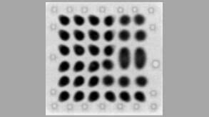
X-ray inspection is a powerful tool for detecting hidden BGA solder joint defects. It enables visualizing shorts, opens, voids, and other anomalies that are not visible from the exterior. 2D and 3D X-ray systems provide valuable insights into the internal joint structure.
-
Are there any industry standards for acceptable BGA solder joint quality?
-
Yes, the IPC-A-610 standard provides acceptance criteria for BGA solder joints. It defines defect categories, target conditions, and inspection methodologies. IPC-7095 is another standard specifically focused on BGA assembly and rework processes.
-
What is the impact of voids on BGA solder joint reliability?
-
Voids reduce the effective cross-sectional area of the solder joint, which can decrease its mechanical strength and thermal conductivity. However, the impact depends on the void size, location, and distribution. IPC-7095 provides guidance on acceptable void levels.
-
How can BGA Rework be performed without damaging the PCB?
- Successful BGA rework requires specialized equipment, skilled operators, and well-defined processes. The key steps are:
- Site preparation by removing the defective component
- Cleaning and reflowing the pads to remove old solder
- Applying fresh solder paste or flux
- Aligning and placing the new component
- Reflowing the new joint using a localized heating method
- Proper temperature control, time management, and ESD precautions are essential to prevent PCB damage during rework.
In conclusion, understanding and controlling BGA soldering defects is crucial for achieving high yields and reliable assemblies. By recognizing the common defect categories, their causes, and prevention methods, manufacturers can optimize their processes to minimize these issues. Regular process monitoring, X-ray inspection, and adherence to industry standards are key tools in this endeavor.


Leave a Reply