1. Solder Paste Application
Solder paste is a mixture of tiny solder particles suspended in flux. It is applied to the PCB pads before placing the components. Proper solder paste application is crucial for achieving good solder joints. Here are some key points to consider:
- Use a stencil with the correct aperture size and shape to ensure the right amount of solder paste is deposited on each pad.
- Maintain the appropriate solder paste viscosity and temperature to achieve consistent application.
- Regularly clean and inspect the stencil to prevent clogging and ensure accurate solder paste deposition.
| Solder Paste Parameter | Recommended Value |
|---|---|
| Viscosity | 800-900 kcps |
| Temperature | 25-30°C |
| Stencil Thickness | 0.1-0.15 mm |
2. Component Placement
Accurate component placement is essential for ensuring proper soldering and preventing defects. Here are some guidelines to follow:
- Use a pick-and-place machine or manual placement tools to accurately position components on the PCB.
- Ensure that the component leads are aligned with the PCB pads and that the components are seated properly.
- Use vision systems or inspection tools to verify the correct placement of components before soldering.

3. Reflow Soldering Profile
Reflow soldering is a process where the PCB assembly is heated in an oven to melt the solder paste and form solder joints. The reflow soldering profile must be carefully controlled to achieve optimal results. Consider the following factors:
- Choose the appropriate reflow profile based on the solder paste and component specifications.
- Maintain the correct peak temperature, time above liquidus (TAL), and cooling rate to ensure proper solder joint formation.
- Monitor the reflow process using thermocouples or profiling systems to ensure consistency and repeatability.
| Reflow Profile Parameter | Lead-Free Solder |
|---|---|
| Peak Temperature | 240-250°C |
| Time Above Liquidus (TAL) | 60-90 seconds |
| Cooling Rate | 2-4°C/second |

4. Flux Selection and Management
Flux is a chemical compound that helps remove oxides from the metal surfaces and promotes solder wetting. Proper flux selection and management are crucial for achieving good solder joints. Consider these points:
- Choose the appropriate flux type (rosin, water-soluble, or no-clean) based on the PCB assembly requirements and cleaning process.
- Ensure that the flux is compatible with the solder paste and the PCB surface finish.
- Regularly monitor and maintain the flux concentration and activity to ensure consistent performance.

5. Solder Joint Inspection
After the soldering process, it is essential to inspect the solder joints to ensure their quality and reliability. Visual inspection is the most common method, but other techniques such as X-ray inspection and electrical testing can also be used. Look for the following characteristics in a good solder joint:
- Smooth and shiny solder surface
- Proper solder joint shape and size
- No visible defects such as bridging, voids, or insufficient solder
- Good wetting and adhesion to the PCB pads and component leads
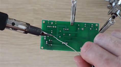
6. Rework and Repair
Despite best efforts, soldering defects may occur, requiring rework or repair. Proper rework techniques are essential to maintain the integrity of the PCB assembly. Follow these guidelines:
- Use the appropriate tools and techniques for component removal, such as desoldering braids, desoldering stations, or hot air rework systems.
- Clean the PCB pads thoroughly before resoldering to ensure good solder joint formation.
- Follow the same soldering guidelines as the initial assembly process, including solder paste application, component placement, and reflow profile.
7. Cleaning
Cleaning the PCB assembly after soldering is essential for removing flux residues and other contaminants that can affect the device’s performance and reliability. Consider these factors:
- Choose the appropriate cleaning method (aqueous, semi-aqueous, or solvent-based) based on the flux type and PCB assembly requirements.
- Ensure that the cleaning process does not damage the components or the PCB substrate.
- Verify the cleanliness of the PCB assembly using visual inspection or contamination testing methods.
8. ESD Protection
Electrostatic discharge (ESD) can damage sensitive electronic components during the soldering process. Implementing proper ESD protection measures is crucial to prevent component failure and ensure the long-term reliability of the device. Follow these guidelines:
- Establish an ESD-safe work environment, including grounded workstations, ESD mats, and wrist straps.
- Use ESD-safe tools and materials, such as conductive tweezers, ESD-safe storage containers, and antistatic packaging.
- Train personnel in ESD awareness and proper handling procedures.
9. Process Control and Monitoring
Implementing process control and monitoring systems is essential for ensuring consistent and reliable soldering results. Consider these aspects:
- Establish a documented soldering process with clear specifications and guidelines.
- Monitor critical process parameters, such as solder paste printing, component placement accuracy, and reflow profile, using appropriate tools and techniques.
- Implement statistical process control (SPC) methods to identify and correct process variations and trends.
10. Training and Skill Development
Investing in the training and skill development of soldering personnel is crucial for achieving high-quality soldering results. Consider these points:
- Provide regular training on soldering techniques, best practices, and new technologies.
- Encourage personnel to obtain relevant certifications, such as IPC-A-610 (Acceptability of Electronic Assemblies) and J-STD-001 (Requirements for Soldered Electrical and Electronic Assemblies).
- Foster a culture of continuous improvement and knowledge sharing among soldering team members.
FAQ
1. What is the difference between lead-based and lead-free solder?
Lead-based solder contains a mixture of tin and lead, while lead-free solder is typically composed of tin, silver, and copper. Lead-free solder has a higher melting point and requires different soldering profiles compared to lead-based solder. The use of lead-free solder is mandated by various environmental regulations, such as RoHS (Restriction of Hazardous Substances).
2. How can I prevent solder bridges during PCB Soldering?
Solder bridges occur when solder inadvertently connects two or more PCB pads or component leads that should not be connected. To prevent solder bridges:
- Ensure proper solder paste application and stencil design
- Maintain accurate component placement
- Optimize the reflow soldering profile
- Use a solder mask to prevent solder from spreading to undesired areas
3. What is the purpose of flux in soldering?
Flux serves several purposes in soldering:
- Removes oxides and contaminants from the metal surfaces to promote solder wetting
- Protects the metal surfaces from oxidation during the soldering process
- Improves the flow and spread of molten solder
- Helps to form a strong and reliable solder joint
4. How do I choose the right solder wire diameter?
The choice of solder wire diameter depends on the soldering application and the size of the components being soldered. Generally:
- Use a thin solder wire (0.5-0.8 mm) for fine-pitch components and small PCB pads
- Use a thicker solder wire (1.0-1.6 mm) for larger components and PCB pads
- Consider the soldering iron tip size and the amount of solder needed for the joint
5. What are some common soldering defects, and how can I prevent them?
Common soldering defects include:
- Solder bridges: Prevented by proper solder paste application, component placement, and reflow profile optimization
- Cold solder joints: Caused by insufficient heat or poor wetting; prevented by maintaining the correct soldering temperature and ensuring clean and oxide-free surfaces
- Solder Voids: Caused by trapped gases or contaminants; prevented by proper flux selection and reflow profile optimization
- Insufficient solder: Caused by inadequate solder paste application or poor wetting; prevented by ensuring the correct solder paste volume and maintaining clean surfaces
- Tombstoning: Caused by uneven heating or component misalignment; prevented by maintaining the correct reflow profile and ensuring accurate component placement
By understanding and addressing these ten critical issues in PCB soldering, manufacturers can achieve high-quality, reliable, and consistent soldering results. Implementing best practices, investing in training, and continuously monitoring and improving the soldering process will help ensure the long-term success and competitiveness of electronics manufacturing operations.


Leave a Reply