Key Components of a PCB Fabrication Drawing
1. Board Outline and Dimensions
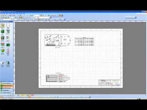
The PCB fabrication drawing should clearly indicate the board outline and dimensions. This information is essential for the manufacturer to determine the size and shape of the PCB. The dimensions should include the length, width, and thickness of the board, as well as any specific features such as cutouts, notches, or rounded corners.
2. Layer Stack-up
The layer stack-up is a critical component of the PCB fabrication drawing. It defines the arrangement of copper layers, insulating materials, and any special layers (such as ground or power planes) that make up the PCB. The stack-up should specify the number of layers, their order, and the thickness of each layer. Additionally, it should include information about the materials used for each layer, such as the type of laminate and copper weight.
3. Drilling and Hole Specifications
The fabrication drawing should provide detailed information about the drilling requirements for the PCB. This includes the location, size, and type of holes needed for components, vias, and mounting. The drawing should specify the drill file format (such as Excellon or Gerber) and the units used (metric or imperial). It should also include any special requirements for hole plating, such as via filling or tenting.
4. Copper Trace and Spacing Requirements
The copper trace and spacing requirements are crucial for ensuring the proper functionality and reliability of the PCB. The fabrication drawing should specify the minimum trace width and spacing for each copper layer, as well as any special requirements for high-current or high-frequency traces. It should also indicate any areas where copper pour or copper thieving is required.
5. Solder Mask and Silkscreen Specifications
The solder mask and silkscreen specifications are important for protecting the PCB and providing visual identification of components and features. The fabrication drawing should include information about the color, thickness, and coverage of the solder mask, as well as any openings or vias that should be exposed. For the silkscreen, the drawing should specify the color, font, and size of the text and graphics, as well as their location on the board.
6. Surface Finish Requirements
The surface finish of the PCB is critical for ensuring proper solderability and protection against oxidation and corrosion. The fabrication drawing should specify the type of surface finish required, such as HASL (Hot Air Solder Leveling), ENIG (Electroless Nickel Immersion Gold), or OSP (Organic Solderability Preservative). It should also include any special requirements for the surface finish, such as the thickness of the plating or the specific alloy composition.
7. Impedance Control Specifications
For high-speed or high-frequency PCBs, impedance control is essential for maintaining signal integrity and reducing electromagnetic interference (EMI). The fabrication drawing should include impedance control specifications, such as the target impedance value, the tolerance, and the specific traces or layers that require impedance control. It should also specify the materials and manufacturing processes required to achieve the desired impedance.
8. testing and Inspection Requirements
The fabrication drawing should include information about the testing and inspection requirements for the PCB. This may include electrical testing, such as continuity and insulation resistance tests, as well as visual inspection for defects or anomalies. The drawing should specify the test methods, acceptance criteria, and any special requirements for testing or inspection.
9. Packaging and Shipping Instructions
Finally, the fabrication drawing should provide instructions for packaging and shipping the manufactured PCBs. This may include specific requirements for moisture barrier bags, desiccants, or other protective materials. It should also specify the labeling and marking requirements for the packaging, as well as any special handling or storage instructions.
Additional Considerations for PCB Fabrication Drawings
In addition to the key components discussed above, there are several other factors to consider when creating a PCB fabrication drawing:
File Formats and Software Compatibility
It is important to ensure that the fabrication drawing is saved in a file format that is compatible with the manufacturer’s software and equipment. Common file formats include Gerber, ODB++, and IPC-2581. It is also a good practice to provide the drawing in a widely accessible format, such as PDF, for easy review and communication.
Revisions and Change Management
As the PCB design evolves, it is crucial to maintain proper revision control and change management for the fabrication drawing. Each revision should be clearly identified and dated, with a description of the changes made. It is also important to communicate any changes to the manufacturer in a timely manner to avoid production delays or errors.
Manufacturability and Design for Manufacturing (DFM)
When creating the fabrication drawing, it is essential to consider the manufacturability of the PCB design. This involves adhering to the manufacturer’s design rules and guidelines, such as minimum trace width and spacing, hole sizes, and clearances. Conducting a DFM review with the manufacturer can help identify and resolve any potential issues before production begins.
Communication and Collaboration
Effective communication and collaboration between the PCB designer, the manufacturer, and other stakeholders are critical for ensuring the success of the project. The fabrication drawing should be reviewed and approved by all relevant parties before production begins. Any questions, concerns, or clarifications should be addressed promptly to avoid delays or misunderstandings.
FAQ
-
What is the purpose of a PCB fabrication drawing?
A PCB fabrication drawing provides the manufacturer with all the necessary information to produce the PCB according to the designer’s specifications. It includes details such as board dimensions, layer stack-up, drilling requirements, and surface finish specifications. -
What file formats are commonly used for PCB fabrication drawings?
Common file formats for PCB fabrication drawings include Gerber, ODB++, and IPC-2581. It is also a good practice to provide the drawing in a widely accessible format, such as PDF, for easy review and communication. -
Why is impedance control important for high-speed or high-frequency PCBs?
Impedance control is essential for maintaining signal integrity and reducing electromagnetic interference (EMI) in high-speed or high-frequency PCBs. The fabrication drawing should include impedance control specifications, such as the target impedance value and the specific traces or layers that require impedance control. -
What is the importance of conducting a DFM review with the manufacturer?
Conducting a DFM (Design for Manufacturing) review with the manufacturer can help identify and resolve any potential issues related to the manufacturability of the PCB design before production begins. This can help avoid production delays, errors, and additional costs. -
How can effective communication and collaboration contribute to the success of a PCB project?
Effective communication and collaboration between the PCB designer, the manufacturer, and other stakeholders are critical for ensuring the success of the project. The fabrication drawing should be reviewed and approved by all relevant parties before production begins, and any questions or concerns should be addressed promptly to avoid delays or misunderstandings.
| Component | Description |
|---|---|
| Board Outline and Dimensions | Specifies the size, shape, and thickness of the PCB, including any specific features such as cutouts or notches. |
| Layer Stack-up | Defines the arrangement of copper layers, insulating materials, and special layers, as well as the thickness and materials used. |
| Drilling and Hole Specifications | Provides information about the location, size, and type of holes needed for components, vias, and mounting. |
| Copper Trace and Spacing Requirements | Specifies the minimum trace width and spacing for each copper layer and any special requirements for high-current or high-frequency traces. |
| Solder Mask and Silkscreen Specifications | Includes information about the color, thickness, coverage, and openings of the solder mask, as well as the color, font, and size of the silkscreen. |
| Surface Finish Requirements | Specifies the type of surface finish required, such as HASL, ENIG, or OSP, and any special requirements for the plating or alloy composition. |
| Impedance Control Specifications | Includes the target impedance value, tolerance, and specific traces or layers that require impedance control for high-speed or high-frequency PCBs. |
| Testing and Inspection Requirements | Specifies the test methods, acceptance criteria, and any special requirements for electrical testing and visual inspection of the PCB. |
| Packaging and Shipping Instructions | Provides instructions for packaging and shipping the manufactured PCBs, including requirements for protective materials, labeling, and handling. |
In conclusion, a comprehensive and well-prepared PCB fabrication drawing is essential for ensuring the successful production of a printed circuit board. By including all the necessary information and considering factors such as manufacturability, file formats, and effective communication, designers can streamline the production process and minimize the risk of errors or delays. A thorough understanding of the key components and best practices for creating PCB fabrication drawings can help designers collaborate effectively with manufacturers and achieve the desired results for their PCB projects.


Leave a Reply