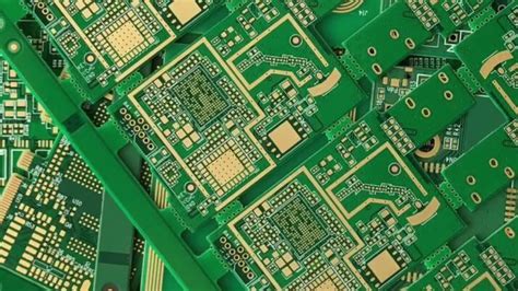
Introduction to Multilayer PCB
A Multilayer PCB, also known as a multilayer printed circuit board, is a complex printed circuit board that consists of multiple layers of conductive copper foil laminated together with insulating material. These layers are interconnected through plated holes called vias, which allow signals to pass from one layer to another. Multilayer PCBs are essential in modern electronics, enabling the creation of compact, high-performance devices with enhanced functionality and reliability.
Advantages of Multilayer PCB
- Space Savings: Multilayer PCBs allow for a higher component density, reducing the overall size of the circuit board and the final product.
- Enhanced Performance: The use of multiple layers enables shorter signal paths, reducing electromagnetic interference (EMI) and improving signal integrity.
- Increased Reliability: Multilayer PCBs offer better protection against environmental factors and mechanical stress, ensuring a longer lifespan for the device.
- Design Flexibility: The multiple layers provide designers with more routing options, allowing for complex circuitry and advanced features.
Multilayer PCB Structure
A typical multilayer PCB consists of the following layers:
- Signal Layers: These layers contain the actual circuit traces that carry electrical signals between components.
- Power Planes: Dedicated layers that provide a low-impedance power distribution network, ensuring stable voltage supply to all components.
- Ground Planes: Layers that serve as a reference for electrical signals and help reduce EMI by providing a low-impedance return path for currents.
- Insulating Layers: Non-conductive layers, typically made of FR-4 material, that separate and insulate the conductive layers.
The number of layers in a multilayer PCB can vary depending on the complexity of the design and the application requirements. Common layer counts include 4, 6, 8, 10, and 12 layers, although some high-end applications may require even more layers.
Layer Stack-up
The arrangement of layers in a multilayer PCB is called the layer stack-up. A well-designed stack-up ensures proper signal integrity, impedance control, and manufacturability. Here’s an example of a typical 6-layer PCB Stack-up:
| Layer | Type | Material | Thickness (mm) |
|---|---|---|---|
| 1 | Signal | Copper | 0.035 |
| 2 | Ground Plane | Copper | 0.035 |
| 3 | Signal | Copper | 0.018 |
| 4 | Signal | Copper | 0.018 |
| 5 | Power Plane | Copper | 0.035 |
| 6 | Signal | Copper | 0.035 |
The choice of material, thickness, and spacing between layers depends on factors such as the desired impedance, signal speed, and manufacturing constraints.

Multilayer PCB Design Considerations
Designing a multilayer PCB involves several key considerations to ensure optimal performance and manufacturability:
Signal Integrity
Signal integrity refers to the ability of a signal to maintain its quality as it propagates through the PCB. To ensure good signal integrity:
- Keep signal traces as short as possible to minimize loss and distortion.
- Maintain consistent impedance throughout the signal path to prevent reflections.
- Use appropriate via sizes and spacing to minimize capacitance and inductance.
- Implement proper termination techniques to reduce ringing and overshoot.
Power Integrity
Power integrity involves providing a stable and clean power supply to all components on the PCB. To achieve this:
- Use dedicated power planes to distribute power evenly across the board.
- Implement proper decoupling capacitors near power-hungry components to suppress noise.
- Minimize the impedance of the power distribution network to reduce voltage drop.
- Use appropriate via sizes and placement to ensure low-impedance connections between power layers.
Electromagnetic Compatibility (EMC)
EMC refers to the ability of a device to operate without causing or being susceptible to electromagnetic interference. To improve EMC:
- Implement proper grounding strategies, such as ground planes and stitching vias.
- Separate sensitive signals from noisy ones using guard traces or shielding.
- Use differential signaling for high-speed signals to reduce EMI.
- Adhere to recommended layout practices, such as avoiding sharp corners and minimizing loop areas.
Thermal Management
As the component density and power consumption of multilayer PCBs increase, thermal management becomes crucial. To ensure proper heat dissipation:
- Use thermal vias to transfer heat from components to the PCB’s copper layers.
- Implement copper pours or dedicated thermal layers to spread heat evenly across the board.
- Consider using high thermal conductivity materials, such as metal-core PCBs, for high-power applications.
- Incorporate appropriate cooling solutions, such as heatsinks or fans, when necessary.

Multilayer PCB Manufacturing Process
The manufacturing process for multilayer PCBs is more complex than that of single or double-layer boards. The general steps involved are:
- Layer Fabrication: Each conductive layer is patterned using photolithography and etching processes.
- Lamination: The individual layers are stacked and laminated together under high temperature and pressure.
- Drilling: Holes are drilled through the laminated board for vias, component leads, and mounting.
- Plating: The drilled holes are plated with copper to create electrical connections between layers.
- Outer Layer Processing: The outer layers undergo additional patterning, solder mask application, and silkscreen printing.
- Surface Finishing: A surface finish, such as ENIG (Electroless Nickel Immersion Gold) or HASL (Hot Air Solder Leveling), is applied to protect the exposed copper and enhance solderability.
- Cutting and Inspection: The panel is cut into individual PCBs, and each board undergoes a final inspection to ensure quality.
The manufacturing process for multilayer PCBs requires specialized equipment and expertise, making it more expensive and time-consuming compared to simpler PCBs.

Applications of Multilayer PCB
Multilayer PCBs find applications in a wide range of industries and products, including:
- Consumer Electronics: Smartphones, tablets, laptops, and wearables.
- Automotive: Advanced driver assistance systems (ADAS), infotainment systems, and electric vehicle power electronics.
- Medical Devices: Implantable devices, diagnostic equipment, and monitoring systems.
- Aerospace and Defense: Avionics, satellite communication systems, and military equipment.
- Industrial Automation: Programmable logic controllers (PLCs), robotics, and process control systems.
- Telecommunications: 5G networks, routers, switches, and base stations.
As technology advances and the demand for smaller, more powerful devices continues to grow, the importance of multilayer PCBs in these industries will only increase.
Frequently Asked Questions (FAQ)
1. What is the difference between a multilayer PCB and a single or double-layer PCB?
A multilayer PCB consists of three or more conductive layers, while single and double-layer PCBs have one or two conductive layers, respectively. Multilayer PCBs offer better space utilization, enhanced performance, and increased design flexibility compared to simpler PCBs.
2. How do vias work in a multilayer PCB?
Vias are plated holes that interconnect different layers of a multilayer PCB. They allow signals to pass from one layer to another, enabling more complex routing and better utilization of board space. Vias can be through-hole (spanning all layers) or blind/buried (connecting only certain layers).
3. What materials are commonly used in multilayer PCBs?
The most common base material for multilayer PCBs is FR-4, a glass-reinforced epoxy laminate. Copper foil is used for the conductive layers, while various solder mask and silkscreen materials are used for protection and labeling. In some cases, specialized materials like high-frequency laminates or metal cores may be used for specific applications.
4. How do I choose the right number of layers for my multilayer PCB?
The number of layers in a multilayer PCB depends on factors such as the complexity of the circuit, the component density, and the signal integrity requirements. Generally, start with the minimum number of layers that can accommodate your design and add layers as needed to improve performance or manufacturability. Consult with your PCB manufacturer for guidance on the most appropriate layer count for your application.
5. What are the challenges in designing and manufacturing multilayer PCBs?
Designing multilayer PCBs involves complex considerations such as signal integrity, power integrity, EMC, and thermal management. Achieving the right balance between these factors while maintaining manufacturability can be challenging. Manufacturing multilayer PCBs requires specialized equipment and expertise, making it more expensive and time-consuming than simpler PCBs. Ensuring proper layer alignment, via formation, and lamination is crucial for the reliability and performance of the final product.
Conclusion
Multilayer PCBs are essential components in modern electronics, enabling the creation of compact, high-performance devices with advanced features and functionality. By understanding the structure, design considerations, and manufacturing process of multilayer PCBs, engineers and designers can create more efficient and reliable products across a wide range of industries.
As technology continues to evolve, the importance of multilayer PCBs will only grow. Staying up-to-date with the latest advancements in materials, design tools, and manufacturing techniques will be crucial for success in this rapidly evolving field.


Leave a Reply