Introduction to PCB Circuit Boards
A Printed Circuit Board (PCB) is the foundation of nearly all modern electronic devices. It provides mechanical support and electrical connections for electronic components using conductive pathways, tracks, or signal traces etched from copper sheets laminated onto a non-conductive substrate.
PCBs have revolutionized electronics manufacturing by providing a reliable and efficient method for mass-producing electronic circuits. They are essential in creating compact, high-performance devices that we use every day, such as smartphones, computers, televisions, and medical equipment.
Key Components of a PCB
- Substrate: The base material on which the circuit is built, typically made from fiberglass or other insulating materials.
- Copper layers: Thin sheets of copper laminated onto the substrate, which are etched to create conductive pathways.
- Solder mask: A protective layer applied over the copper traces to prevent short circuits and provide insulation.
- Silkscreen: Text and symbols printed on the PCB to identify components and provide assembly instructions.
- Vias: Conductive holes drilled through the board to connect different layers of the PCB.
- Pads: Exposed areas of copper used for soldering components to the board.
Types of PCB Boards
PCBs can be classified based on the number of layers, the materials used, and their manufacturing process. Understanding the different types of PCBs is crucial for selecting the right board for your project.
Single-sided PCBs
Single-sided PCBs have conductive traces on only one side of the substrate. They are the simplest and most cost-effective type of PCB, suitable for low-complexity circuits and prototyping.
Double-sided PCBs
Double-sided PCBs have conductive traces on both sides of the substrate, allowing for more complex circuits and higher component density. Vias are used to connect the traces on the top and bottom layers.
Multi-layer PCBs
Multi-layer PCBs consist of three or more conductive layers separated by insulating layers. They offer the highest component density and are used in complex, high-performance devices.
| PCB Type | Layers | Cost | Complexity | Applications |
|---|---|---|---|---|
| Single-sided | 1 | Low | Low | Simple circuits, prototyping |
| Double-sided | 2 | Medium | Medium | More complex circuits |
| Multi-layer | 3+ | High | High | High-performance devices |
Rigid PCBs
Rigid PCBs are made from a solid, inflexible substrate material, such as FR-4. They are the most common type of PCB and are used in a wide range of applications.
Flexible PCBs
Flexible PCBs (FPCBs) are made from a flexible substrate material, such as polyimide. They can bend and twist without damaging the circuit, making them ideal for applications with limited space or requiring movement.
Rigid-Flex PCBs
Rigid-Flex PCBs combine the features of rigid and flexible PCBs, consisting of both rigid and flexible sections. They offer the benefits of both types of boards and are used in applications requiring a combination of stability and flexibility.
PCB Design and Manufacturing Process
Designing and manufacturing a PCB involves several steps, each crucial for ensuring the board’s functionality, reliability, and manufacturability.
PCB Design Steps
- Schematic capture: Creating a schematic diagram of the circuit using EDA (Electronic Design Automation) software.
- Component placement: Arranging the components on the board to optimize space and minimize signal interference.
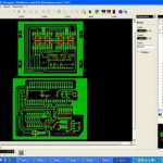
- Routing: Connecting the components using conductive traces while adhering to design rules and constraints.
- Design rule check (DRC): Verifying that the design meets the manufacturing specifications and design rules.
- Gerber file generation: Exporting the design files in a format compatible with PCB manufacturing equipment.
PCB Manufacturing Process
- PCB Fabrication:
- Printing the circuit pattern onto the copper-clad laminate
- Etching away the unwanted copper
- Drilling holes for vias and component leads
- Applying solder mask and silkscreen
- PCB Assembly:
- Solder paste application
- Component placement
- Reflow soldering
- Inspection and testing

Choosing the Right PCB for Your Project
Selecting the appropriate PCB for your project depends on several factors, including:
- Circuit complexity
- Environmental conditions (temperature, humidity, vibration)
- Power requirements
- Size constraints
- Cost
Consider the following guidelines when choosing a PCB:
- Use single-sided or double-sided PCBs for simpler circuits and prototypes
- Opt for multi-layer PCBs for complex, high-performance devices
- Choose rigid PCBs for most applications, and flexible or rigid-flex PCBs for space-constrained or moving parts
- Ensure the PCB material is suitable for the environmental conditions
- Balance cost and performance based on your project requirements
Common PCB Design Mistakes to Avoid
- Incorrect component footprints
- Violating design rules (e.g., minimum trace width, clearance)
- Poor component placement and routing
- Inadequate power and ground distribution
- Neglecting signal integrity and EMI/EMC considerations
To avoid these mistakes:
- Double-check component footprints and datasheets
- Familiarize yourself with the design rules for your chosen manufacturing process
- Use EDA software with built-in DRC tools
- Follow best practices for component placement, routing, and power distribution
- Consider signal integrity and EMI/EMC early in the design process
Frequently Asked Questions (FAQ)
1. What is the difference between a PCB and a breadboard?
A breadboard is a prototyping tool used for temporarily building and testing electronic circuits without soldering. PCBs, on the other hand, are permanent boards that provide mechanical support and electrical connections for electronic components.
2. How do I choose the right PCB manufacturer?
When selecting a PCB manufacturer, consider factors such as:
- Manufacturing capabilities (e.g., layer count, materials, minimum feature sizes)
- Quality control processes
- Lead times and pricing
- Customer support and communication
- Certifications (e.g., ISO, UL, RoHS)
3. What is the typical turnaround time for PCB manufacturing?
Turnaround times vary depending on the complexity of the board, the manufacturer’s workload, and the shipping method. Standard lead times range from 1-2 weeks for simple boards to 4-6 weeks for complex, multi-layer boards.
4. How much does it cost to manufacture a PCB?
The cost of manufacturing a PCB depends on several factors, including:
- Board size and thickness
- Number of layers
- Material
- Quantity
- Surface finish and special requirements
Prices can range from a few dollars for simple, single-sided boards to hundreds of dollars for complex, multi-layer boards.
5. What is the minimum feature size for PCB traces and spaces?
The minimum feature size depends on the PCB manufacturer’s capabilities and the chosen manufacturing process. Typical minimum trace widths and spaces range from 3-6 mils (0.003-0.006 inches) for standard PCBs, while advanced processes can achieve feature sizes as small as 1-2 mils.
Conclusion
In this comprehensive guide, we have covered the essential aspects of PCB circuit boards, including their components, types, design, and manufacturing processes. We have also provided guidance on choosing the right PCB for your project and avoiding common design mistakes.
By understanding the fundamentals of PCBs and following best practices throughout the design and manufacturing process, you can create reliable, high-performance electronic devices that meet your project requirements.
Remember to work closely with your chosen PCB manufacturer, adhere to design rules and guidelines, and consider factors such as circuit complexity, environmental conditions, and cost when selecting the appropriate PCB for your project.
Leave a Reply